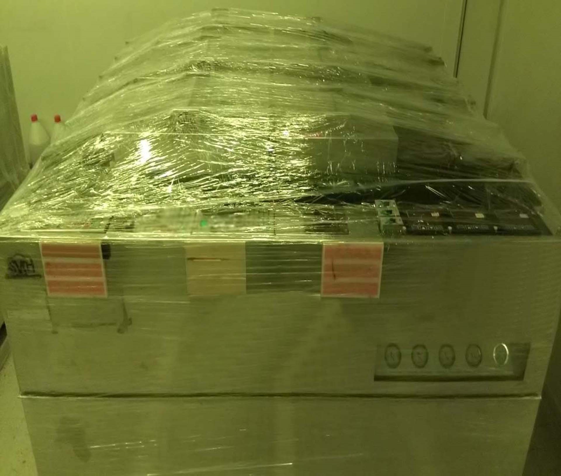
Used SVG 860 #9238247 for sale
URL successfully copied!
Tap to zoom


SVG 860 is an advanced photoresist equipment from Nikon Instruments Ltd. used for image transfer and patterning in microelectromechanical systems (MEMS) device fabrication. It is an integrated deposition, spin-coating and exposure tool designed for a variety of materials such as polysilicon, polyimide, and negative resist. 860 is based on state-of-the-art imaging technology and is equipped with a high NA (numerical aperture) optical immersion system, a high-precision stage, an air bearing spinner inclitator, and an advanced lighting unit. It also offers an array of coating parameters that can be finely tuned, to ensure that precise thin film properties are achieved. The machine relies on a two-stage spin coating process, with deposition and exposure occurring in separate steps. The first step is deposition, where a precise amount of photoresist material is applied to the substrate surface. Then, the substrate is spun at precise speeds, to create an even, thin film. After the spinning process, the substrate is moved to the second stage for exposure. In the exposure stage, light from the optical immersion tool is shone onto the substrate and accurately patterned. The biological photoresist layer is then selectively removed or changed depending on the exposure conditions. This method of exposure creates a variety of precisely shaped features with excellent resolution. SVG 860 also allows for inline inspection and measurement of the photoresist film thickness on the test chips. This allows manufacturers to measure the thickness of the film without tearing down and cleaning the chamber, accelerating the process and increasing throughput. The photoresist asset is designed to be compatible with high volume lithography processes in semiconductor and MEMS manufacturing, due to its precision, precision control and easy operation. The model is engineered for reliability and requires minimal maintenance for improved productivity. This advanced photoresist equipment ensures the creation of features on MEMS chips with high accuracy, resolution, and repeatability.
There are no reviews yet