Used SVG MS III+ #293762270 for sale
URL successfully copied!










Tap to zoom
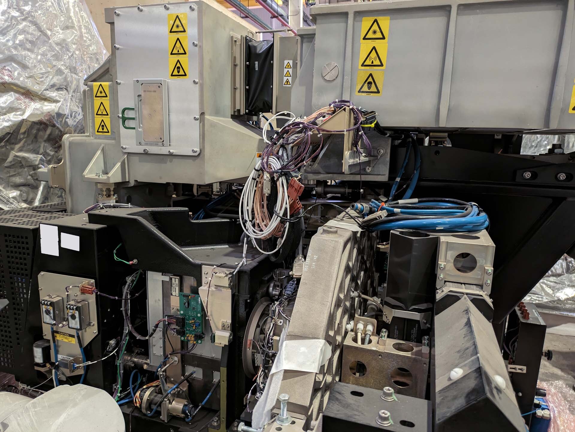

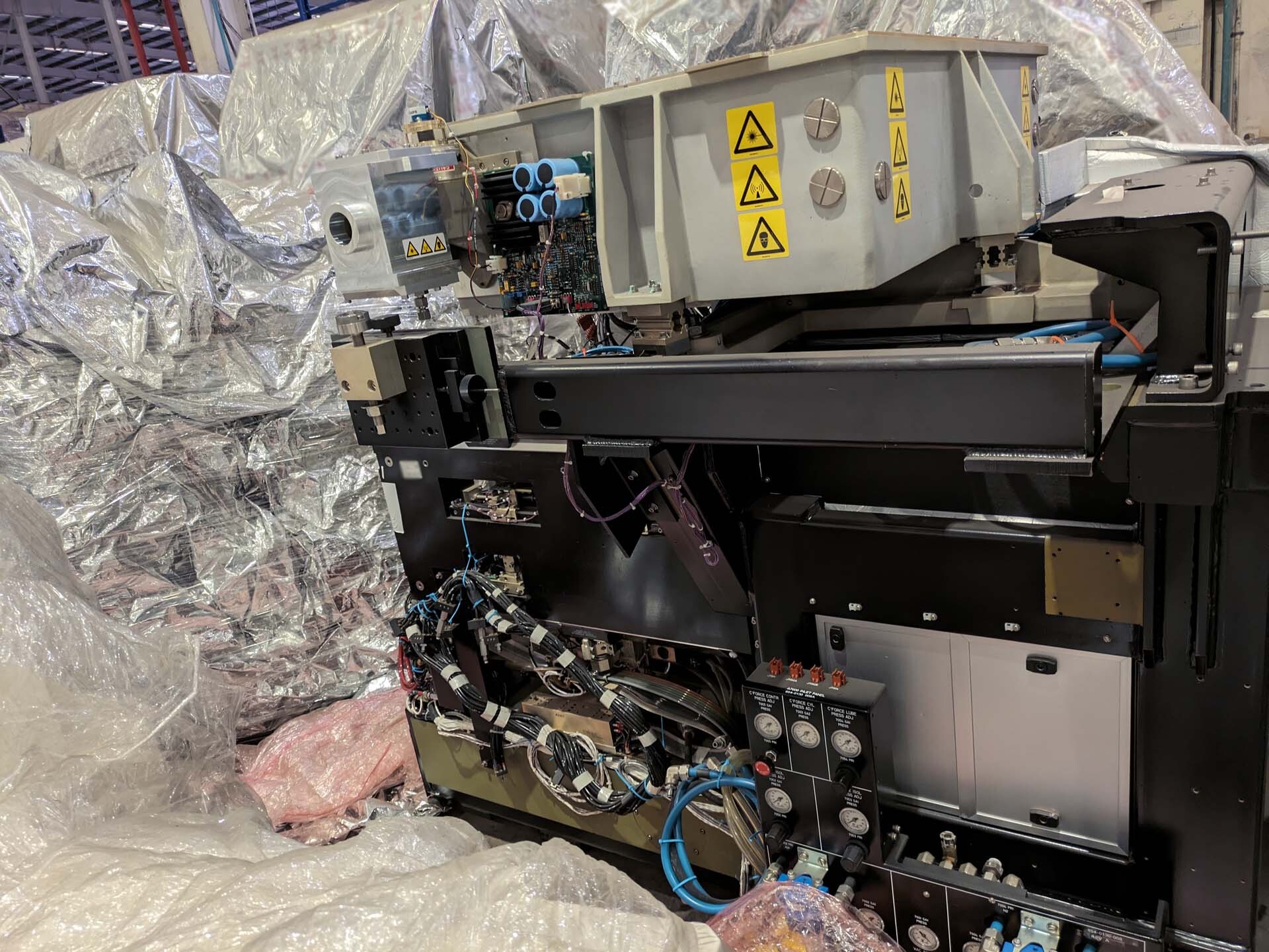
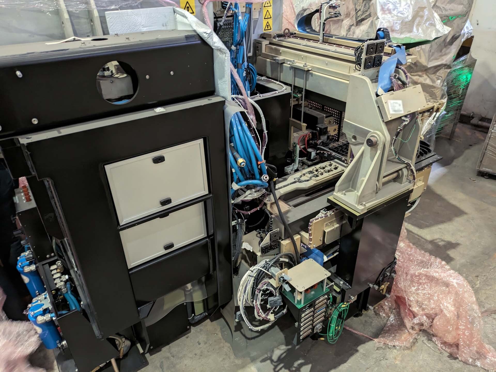

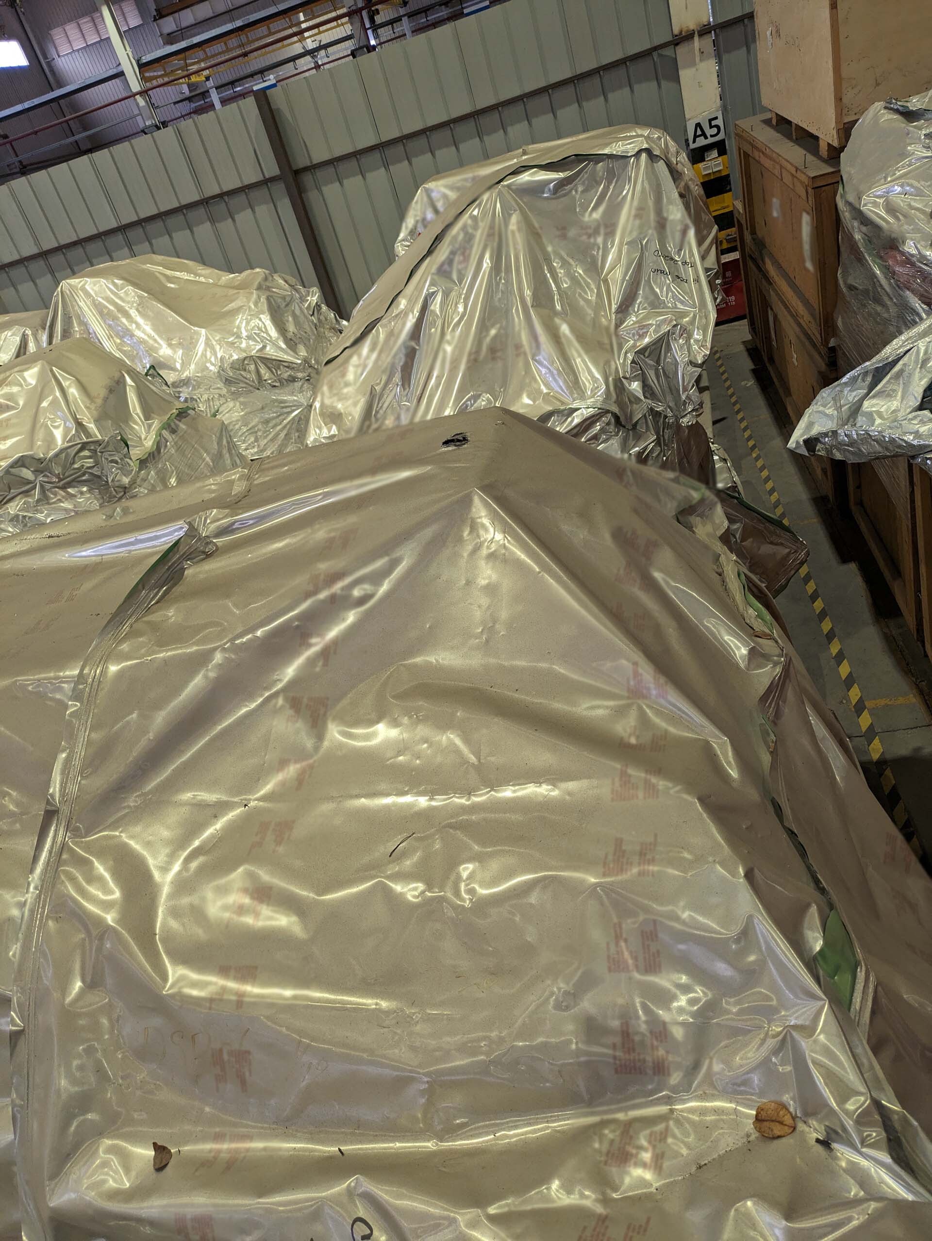
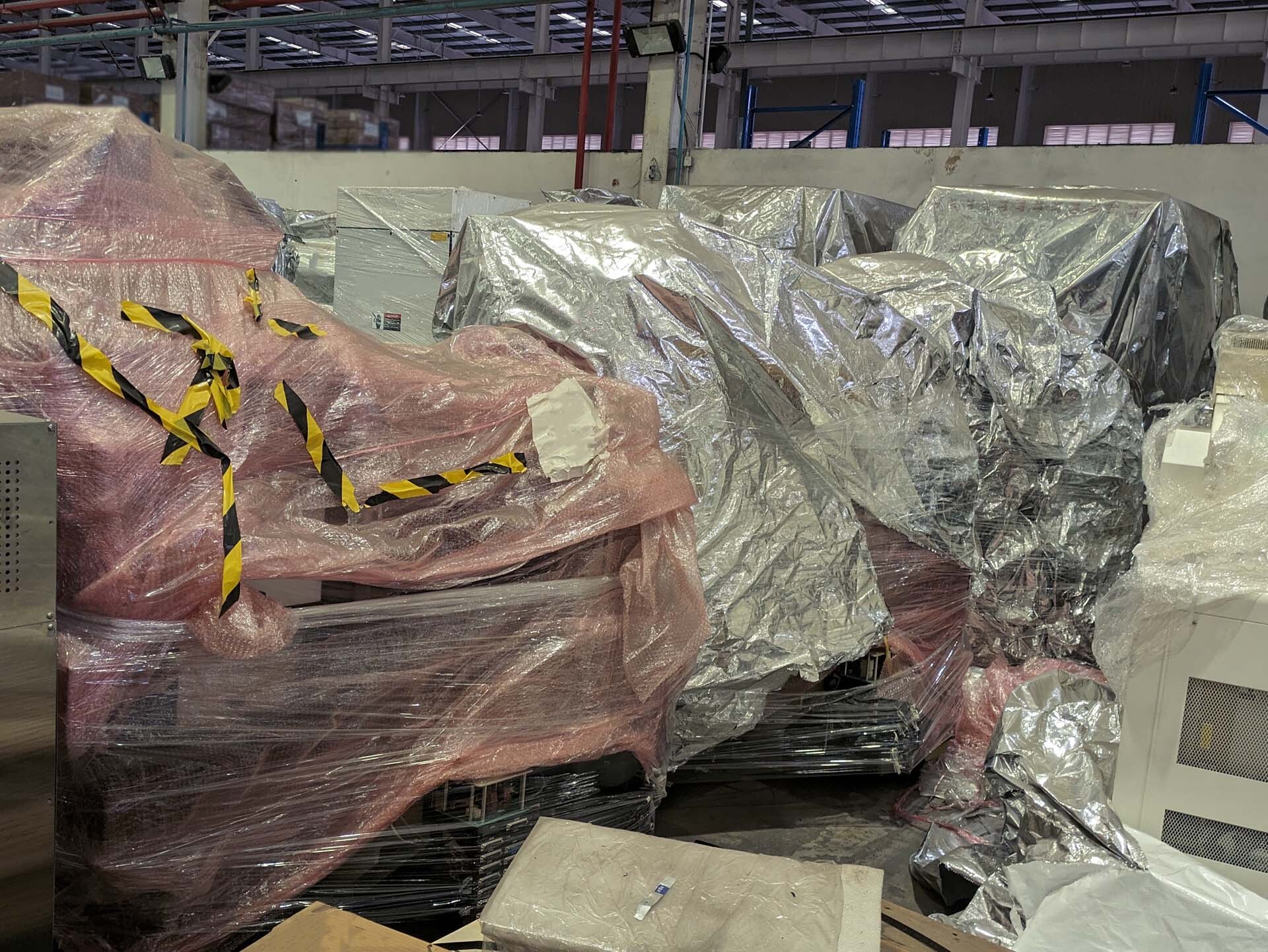
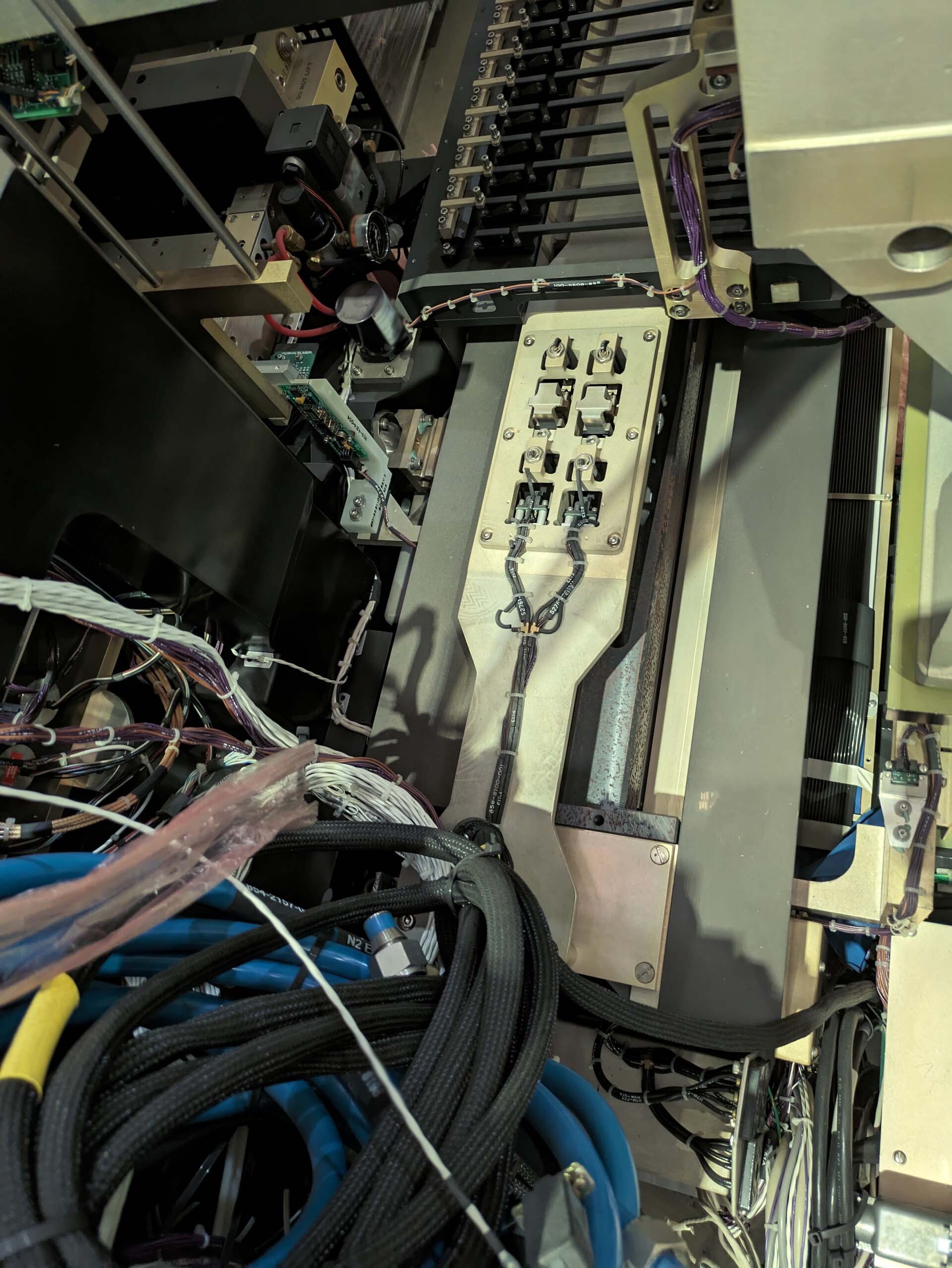
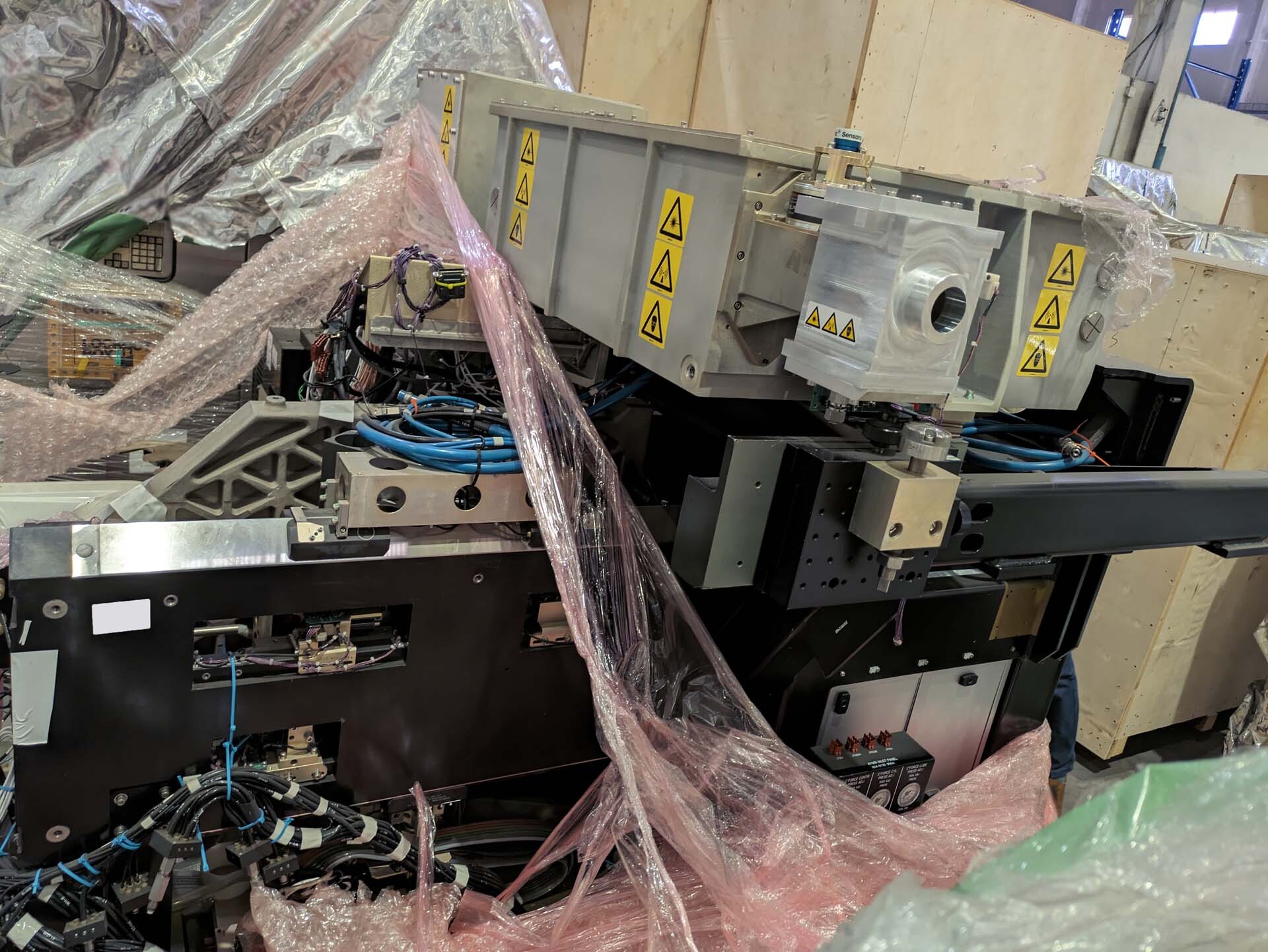
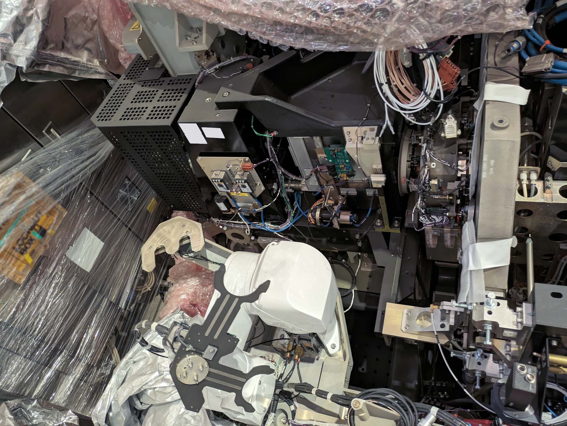
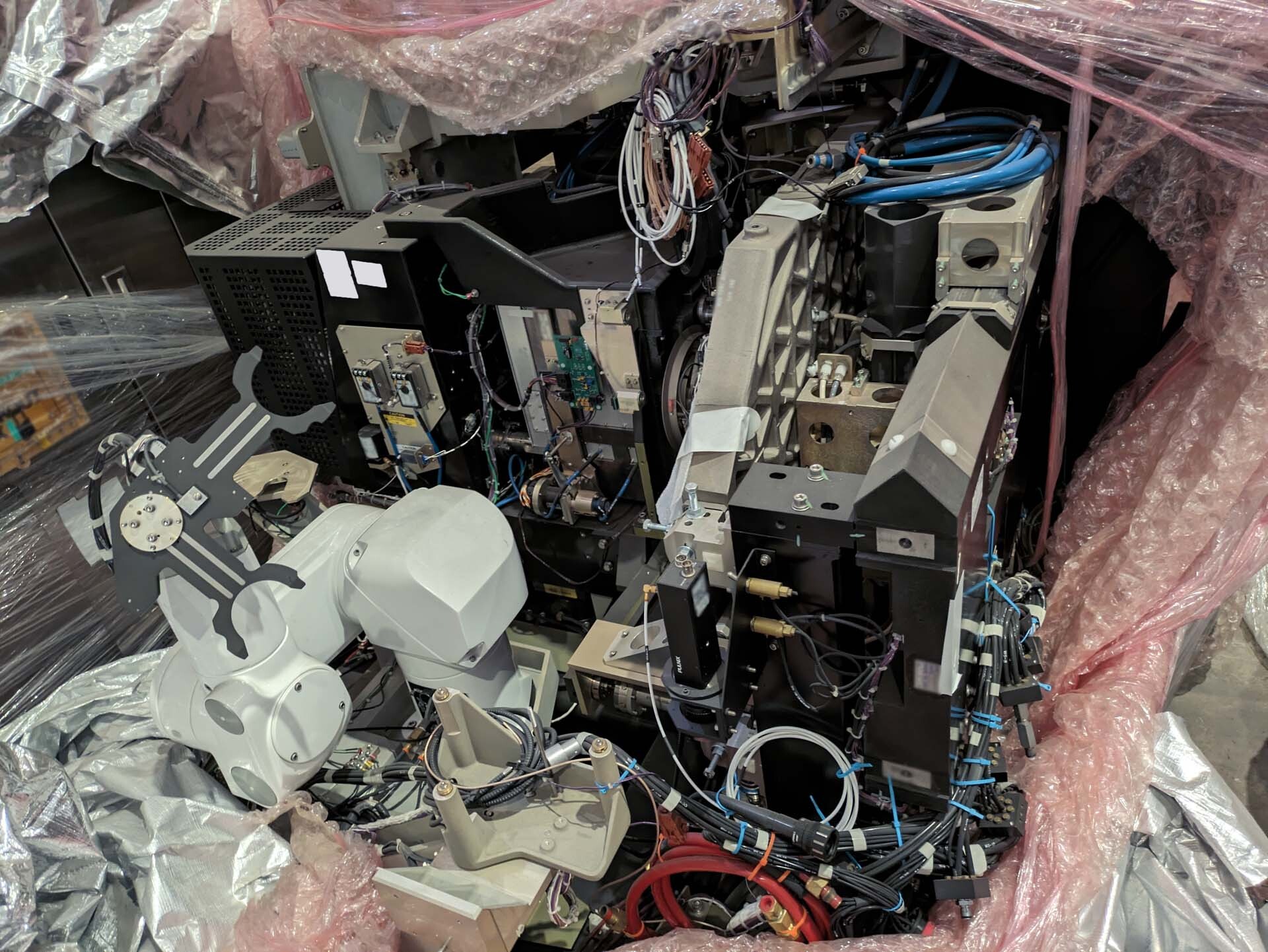
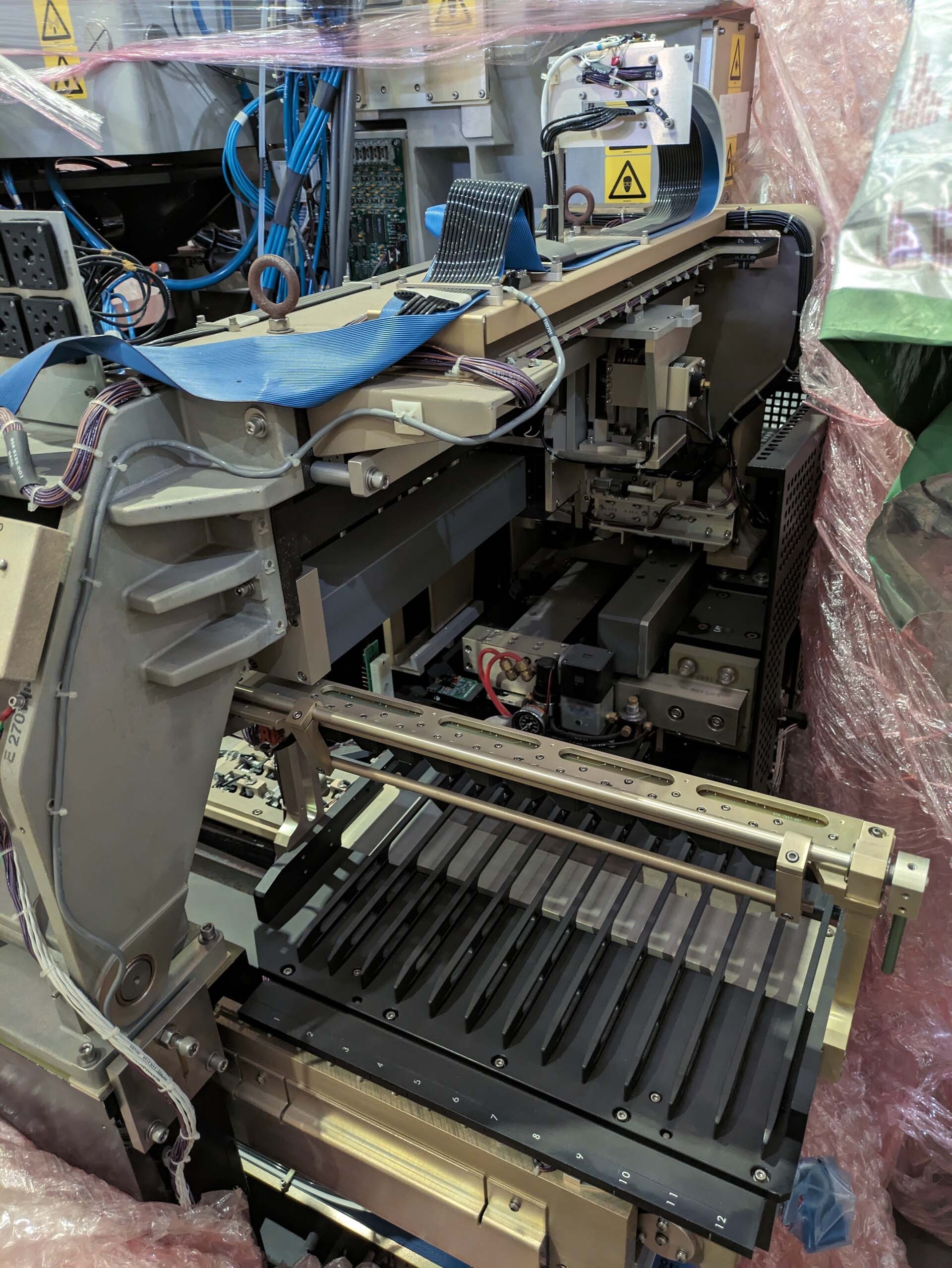


SVG MS III+ is a cutting-edge photolithography equipment specifically designed for advanced semiconductor manufacturing processes. As a critical component in the fabrication of integrated circuits (ICs), photoresist systems like MS III+ play a crucial role in defining patterns on semiconductor substrates with unrivaled precision and accuracy. This system is renowned for its exceptional resolution, throughput, and reliability, making it a preferred choice for leading semiconductor manufacturers worldwide. At the heart of SVG MS III+ unit is its sophisticated exposure mechanism, which employs state-of-the-art optics and projection technologies to transfer intricate patterns from photomasks onto semiconductor wafers. This process is critical in defining the layout of various circuit elements on the wafer, such as transistors, capacitors, and interconnects, with sub-micron resolution. The machine's high-resolution imaging capabilities are essential for achieving the tight dimensional tolerances and feature sizes demanded by advanced semiconductor designs. One of the key strengths of MS III+ tool is its versatility and adaptability to different process requirements. With advanced control algorithms and customizable exposure parameters, the asset can accommodate a wide range of photoresist materials, including positive, negative, and chemically amplified resists. This flexibility allows semiconductor manufacturers to tailor the lithography process to the specific needs of their device designs, ensuring optimal pattern fidelity and uniformity across the wafer. In addition to its superior imaging capabilities, SVG MS III+ model offers industry-leading throughput and efficiency, enabling high-volume production of semiconductor devices with reduced cycle times and increased yield. The equipment's advanced wafer handling mechanisms, robotic interfaces, and automated alignment systems streamline the lithography process, minimizing downtime and maximizing productivity. This high throughput is essential for meeting the demanding production schedules of modern semiconductor fabs and ensuring cost-effective manufacturing operations. Furthermore, MS III+ system incorporates advanced monitoring and control features to ensure consistent and reproducible patterning results across multiple wafers and process runs. Real-time process feedback mechanisms, integrated metrology tools, and automated error detection algorithms enable operators to monitor and optimize lithography performance, identify potential issues, and implement corrective actions promptly. This proactive approach to unit management helps maintain process stability, reduce defects, and improve overall yield in semiconductor manufacturing. Moreover, SVG MS III+ machine is designed with scalability and future-proofing in mind, allowing semiconductor manufacturers to upgrade and expand the tool capabilities as technology progresses. The asset's modular architecture, upgradable components, and compatibility with emerging lithography techniques ensure long-term compatibility with evolving semiconductor processes and device designs. This scalability is essential for semiconductor fabs seeking to stay at the forefront of innovation and maintain a competitive edge in the dynamic semiconductor industry. In conclusion, MS III+ photoresist model represents a pinnacle of photolithography technology, offering unparalleled resolution, throughput, and reliability for advanced semiconductor manufacturing applications. With its cutting-edge imaging capabilities, process flexibility, and advanced control features, SVG MS III+ equipment enables semiconductor manufacturers to achieve the highest levels of precision and efficiency in patterning semiconductor devices, driving innovation and excellence in the semiconductor industry.
There are no reviews yet