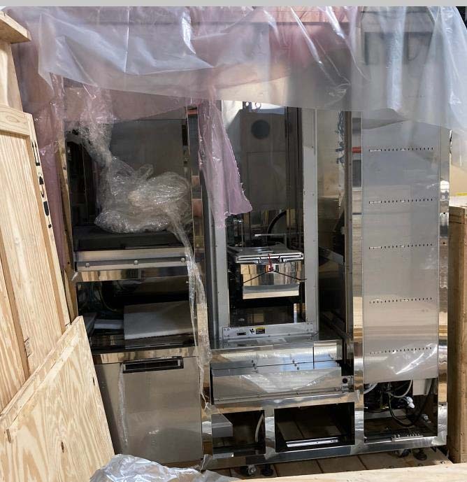
Used TEL / TOKYO ELECTRON ACT 12 #293597470 for sale
It looks like this item has already been sold. Check similar products below or contact us and our experienced team will find it for you.
Tap to zoom


Sold
ID: 293597470
System, parts machine
Uninterruptible Power Supply (UPS)
(2) T/H Filters
TCU Controller missing
PRB 1:
No module
No spin station
PRB 2:
(4) CPLs
DEV
REX Controller
(4) CHP Modules, 12"
(4) HHPs, 12"
(5) CPLs, 12"
(2) TRS Modules
(3) Combustible gas monitoring boxes
MICROBAR Mini wastemate controller
HMDS: Solvent Slender Chemical Cabinet (SSCC)
RDS Pump drawers with drain manifolds
CRA / IRA:
Head missing
Theta
Y, Z-Axis
HFA Block:
PRA
Sentry controllers.
TEL / TOKYO ELECTRON ACT 12 is a photoresist equipment manufactured by TEL Limited (TOKYO ELECTRON), a leading global supplier of semiconductor production equipment. It is a critical component of the semiconductor manufacturing process and is used to precisely etch semiconductor devices. TEL ACT 12 system is capable of performing a variety of photolithography processes and supports a wide range of resist materials for use in various semiconductor production applications. TOKYO ELECTRON ACT12 unit utilizes advanced high-resolution imaging optics coupled with an automated wafer alignment machine to provide precise alignment of the wafer with the photomask. This ensures the patterns printed on the photomask are accurately transferred to the wafer surface for subsequent etching. The tool's high resolution optics also provide superior control of the resist thickness and etch depth, leading to improved yields and device performance. The asset is comprised of several subsystems, each designed to optimize a specific stage of the photolithography process. The Resist Processing Model (RPS) is responsible for cleaning and baking the wafer as well as applying the photoresist, while the Photomask Alignment Equipment (PAS) is in charge of aligning the photomask with the wafer. The Photoresist Transfer System (PTS) is responsible for imaging the photomask onto the wafer and transferring the pattern to the photoresist, while the Exposure Control Unit (ECS) ensures the proper exposure parameters are met. The machine is also equipped with TEL / TOKYO ELECTRON patented ActiveSite™ Inspection and Process Monitoring Tool, which provides feedback and control of pattern transfer processes in real-time to ensure repeatable, high-quality product production. The asset is surrounded by a sophisticated environmental control chamber, designed to keep the model free from dirt and other contaminants, enabling maintenance-free operation for extended periods of time. In addition to being highly reliable and automated, ACT 12 equipment also provides an exceptionally large process window. This enables the system to handle a wide range of wafer sizes from 150 to 450 mm and a wide range of resist types, making it suitable for use in a variety of semiconductor applications. Lastly, its modular design and upgradable architecture allow for easy customization of the unit, making it well-suited to address the unique requirements of each semiconductor fabrication line.
There are no reviews yet