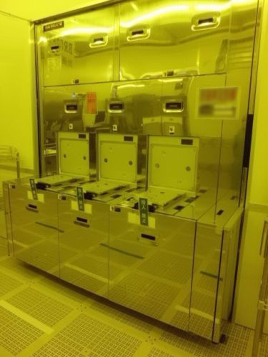
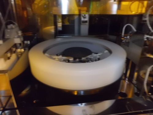
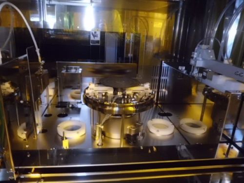
Used TEL / TOKYO ELECTRON ACT 12 #9102945 for sale
URL successfully copied!
Tap to zoom










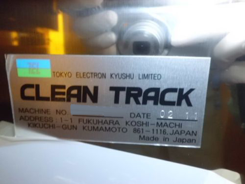

ID: 9102945
Wafer Size: 12"
Vintage: 2002
(3) Coaters / (4) Developers systems, 12"
2002 vintage.
TEL / TOKYO ELECTRON ACT 12 is a photoresist equipment used in etching and patterning of semiconductors and thin-film materials in the production of integrated circuits and other electronic components. This system allows for precise and accurate patterning of the thin-film materials in the desired shape. It is designed to provide excellent performance in photolithography processes and is capable of producing high-resolution patterns with minimum substrate damage. TEL ACT 12 unit is composed of several components, including a light source, lens, aperture, and scanner. The light source is a multi-wavelength UV light source that produces a uniform light beam for uniform exposure of the substrate. The lens is designed to provide a larger field of view and improve upon resolution for clean pattern execution. The aperture is used to shape the light source for uniform and precise patterning. The scanner is also designed to provide a large-area scanning field for quick and accurate patterning. The basic etching process of TOKYO ELECTRON ACT12 machine follows a sequential pattern. First, the photoresist is spun onto the substrate. This process needs to be well-controlled in order to obtain the desired etch pattern. This is done by adjusting the viscosity, spin speed, and temperature of the photoresist before it is applied. Second, the substrate is exposed to the UV light source. The light beam is focused and shaped by the lens and aperture to achieve precise patterning. Third, the photoresist is developed and is patterned on the substrate in the desired shape. Finally, the substrate is etched to create the desired pattern. ACT 12 tool is a reliable and efficient industrial photolithography tool. Its precision patterning capabilities provide the highest standard of quality for efficient production of semiconductor and thin-film components. Additionally, its large scanning field and multi-wavelength light source makes it an ideal tool for use in etching and patterning of a variety of materials. Overall, TOKYO ELECTRON ACT 12 asset is an effective photoresist model for the etching and patterning of integrated circuits and other components in the electronics industry.
There are no reviews yet

