Used TEL / TOKYO ELECTRON ACT 12 #9105213 for sale
URL successfully copied!
Tap to zoom

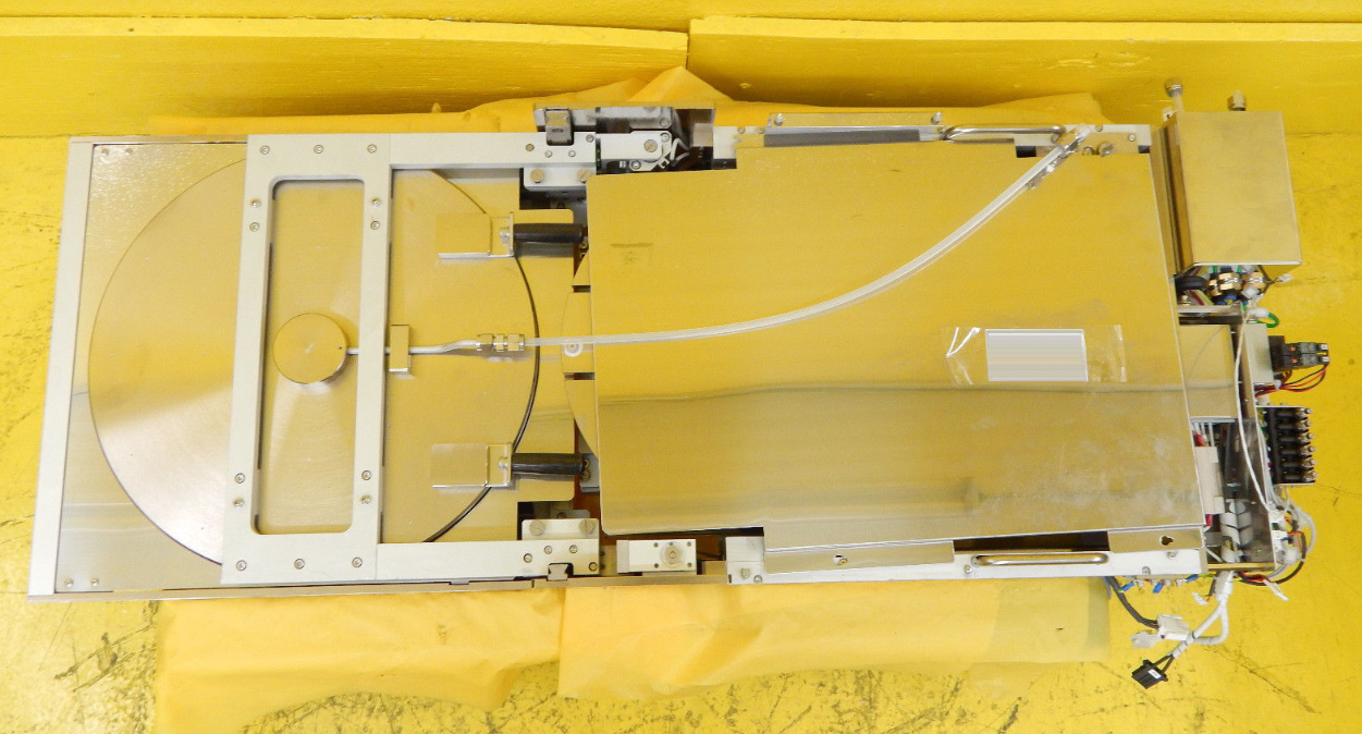

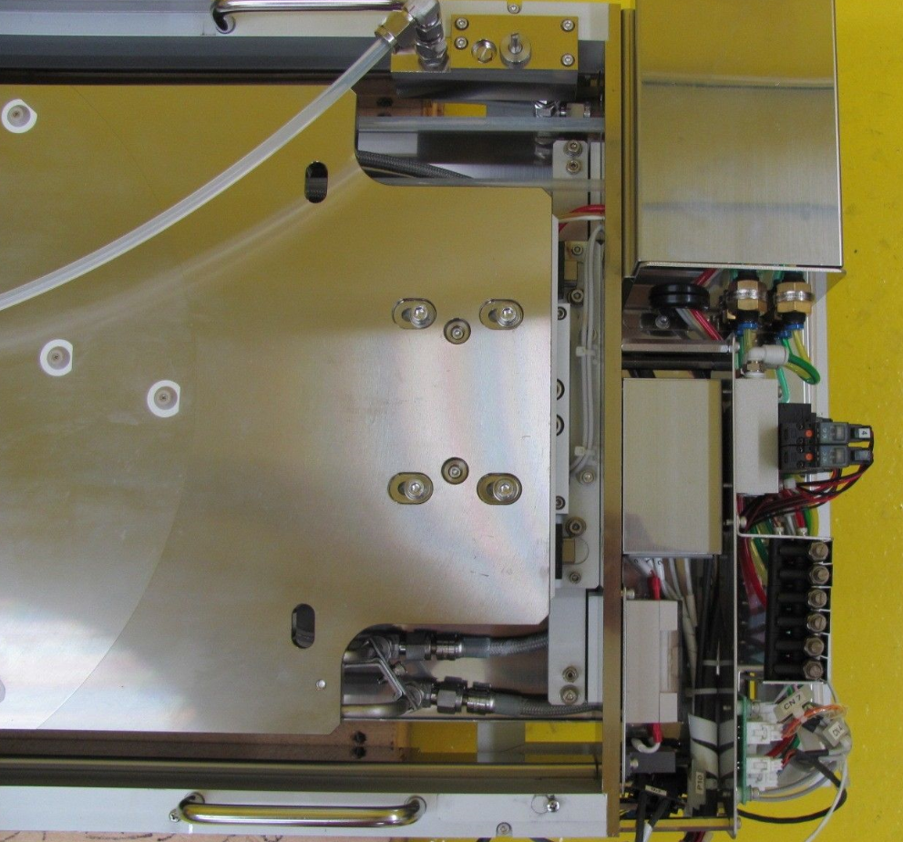

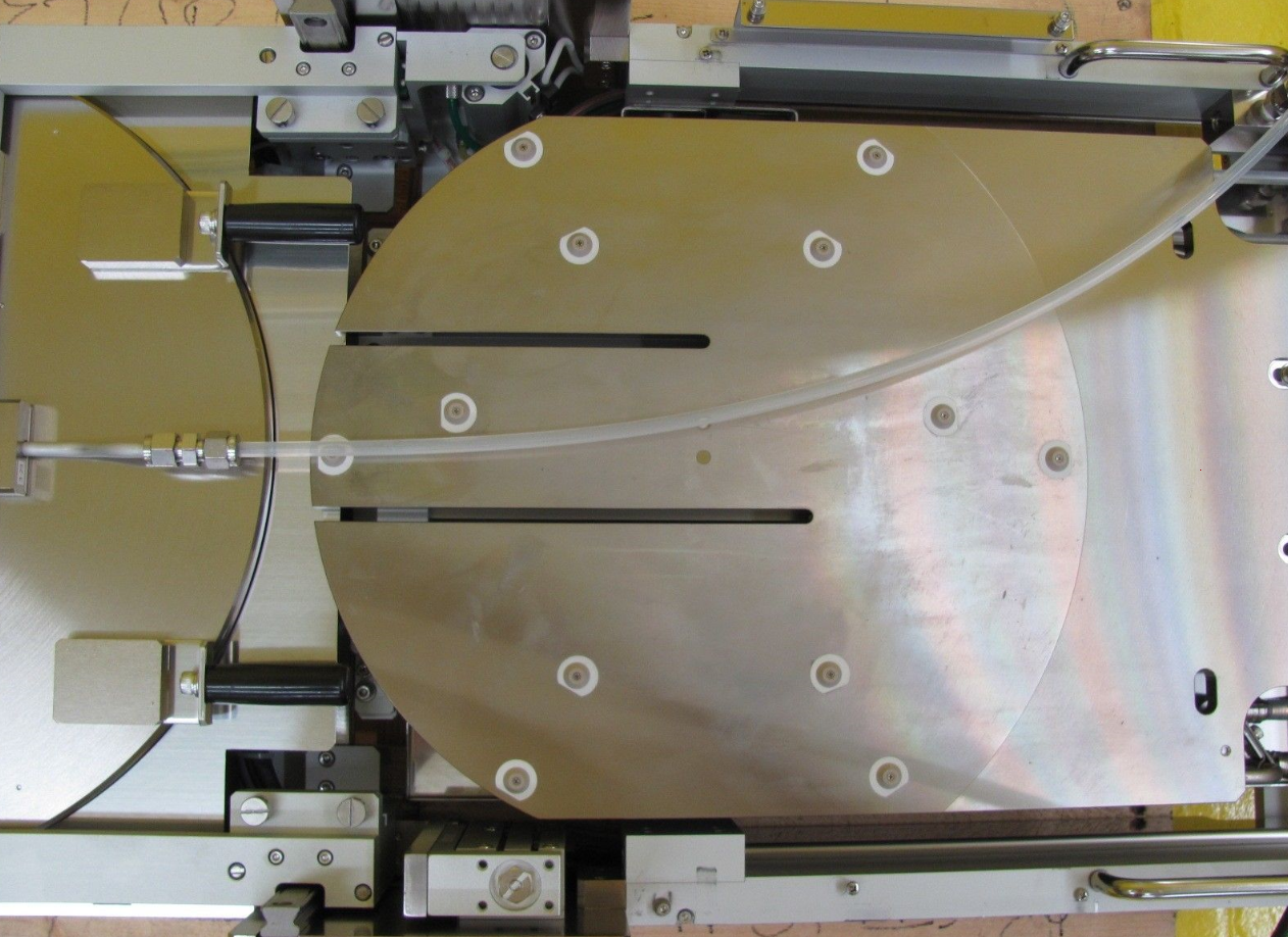


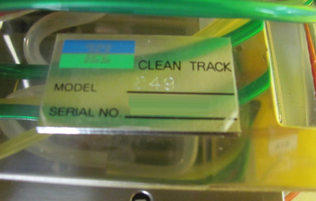

ID: 9105213
Wafer Size: 8"
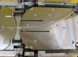
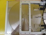
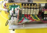
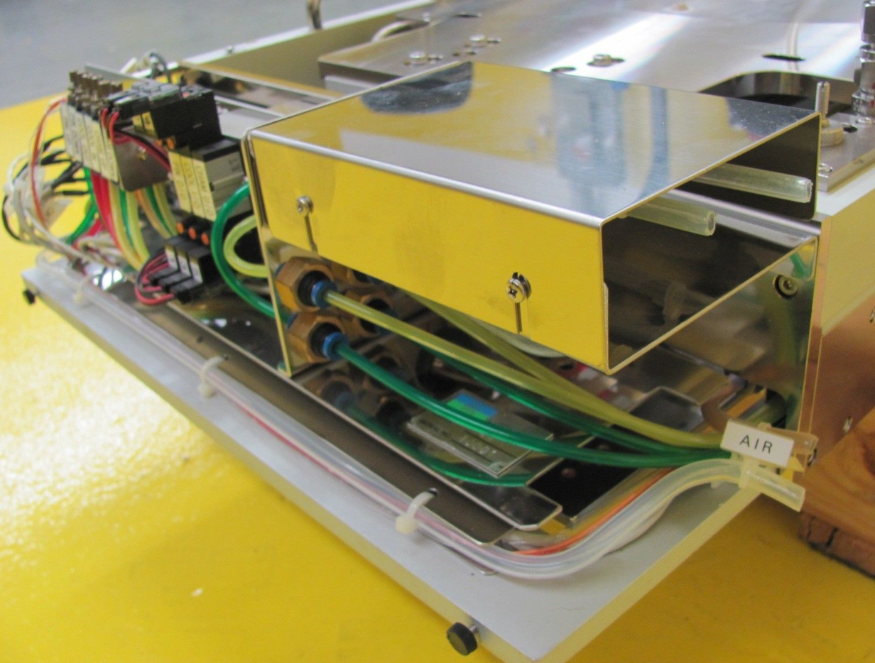
Chilling hot plate process station, 8"
2985-41180-w6 CHP PEB SUB UNIT Assy
2985-437216-w8 Base (ACT 12-CHP) Assy Col
2980-091282-12 Col Plate AT12-SP-NDK
2985-410708-W2 CHP Plate Support Assy
2985-411097-W1 CHP Chamber Assy
2980-091282-12 Col Plate AT12-CP-NDk.
TEL / TOKYO ELECTRON ACT 12 is a photoresist system that is used in lithography processes within the semiconductor industry. It is a vapor phase deposition technique for depositing a thin layer of photoresist material onto a substrate such as silicon or glass. The technology works by combining a liquid monomer, sensitizer, solid filler, and diluent to create a suspension of photoresist material. This suspension is then applied to the substrate through a sprayer or via spin coating techniques. Once the photoresist coating is ensured to be uniform, it is cured so that it adheres to the substrate. Once the photoresist layer is cured and adhered to the substrate, the material is radiation sensitive. TEL ACT 12 uses a short pulse of lower UV energy, typically in the form of a built-in laser source, to cause exposure of the photoresist to the activated radiation source. The underlying patterning of the substrate now serves as a mask to determine the imaging resolution of the resist development. The photoresist is developed using a chemical development process that changes the soluble areas of the photoresist to the insoluble areas. Besides this, positive and negative photoresists can be used depending upon the needs of the lithographic process. TOKYO ELECTRON ACT12 is commonly used in semiconductor processing as a method for patterning layer geometries and features. This allows for the transfer of pre-defined images onto a semiconductor in a way that can be replicated accurately and reliably. It is also commonly used for process diagnostics such as checking the alignment of patterns during the lithography process. ACT 12 process is capable of precise control over pattern fidelity. Complex images can be created using this technology, especially when coupled with optical lithography. The process is also able to create very thin films that are resistant to the exposure to various types of radiation, heat, and chemicals. Additionally, the process provides an environmentally friendly photoresist system in terms of reduced volatile organic compound (VOC) emissions. In conclusion, TEL ACT12 photoresist system provides a reliable and efficient way to create lithographic patterns with precision. It is durable and resistant to radiation, heat, and chemicals ensuring that patterns remain in tact during processing and also provides an environmentally friendly option in terms of VOC emissions.
There are no reviews yet


