Used TEL / TOKYO ELECTRON ACT 12 #9112086 for sale
URL successfully copied!
Tap to zoom






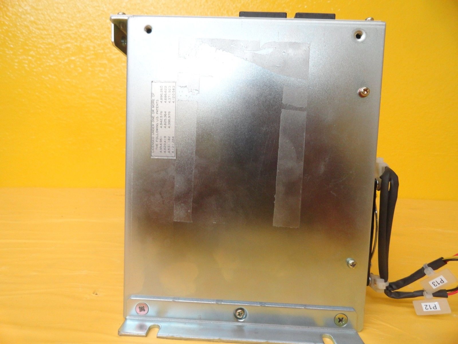

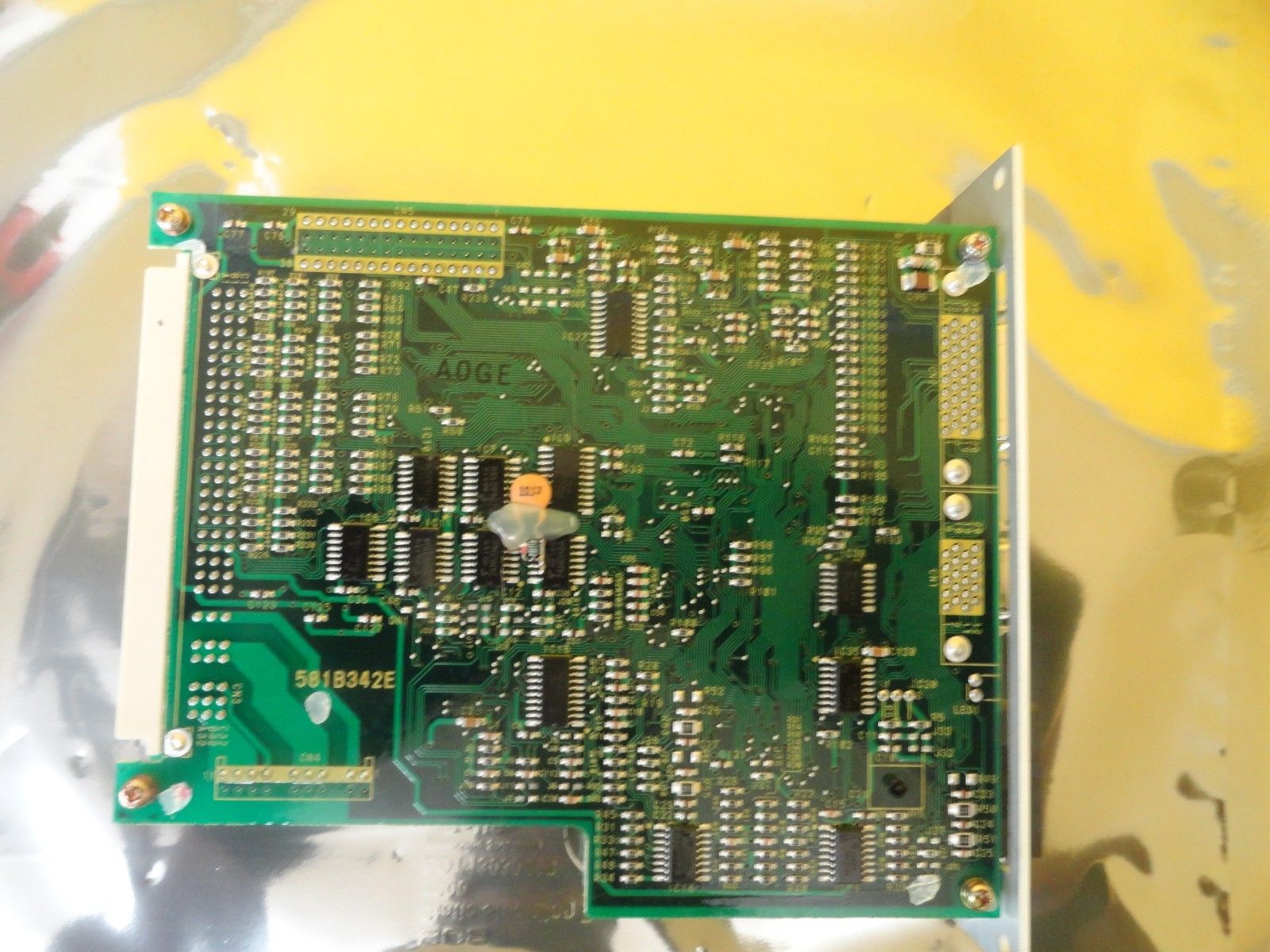

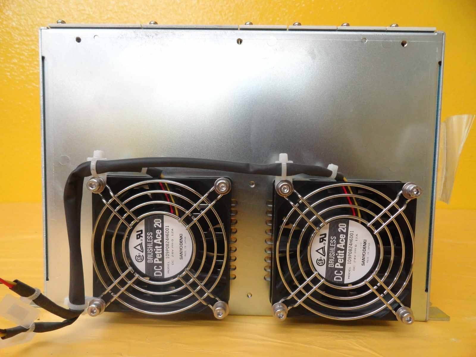

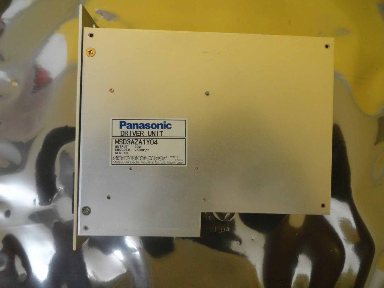

ID: 9112086
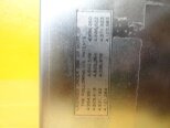
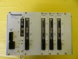
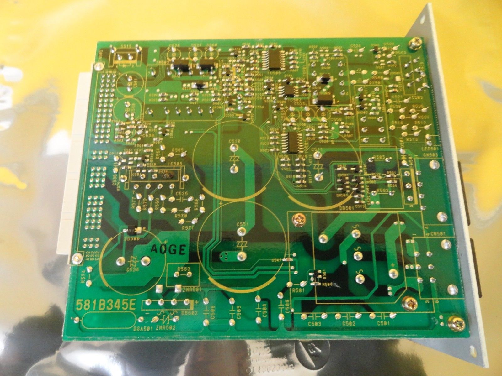
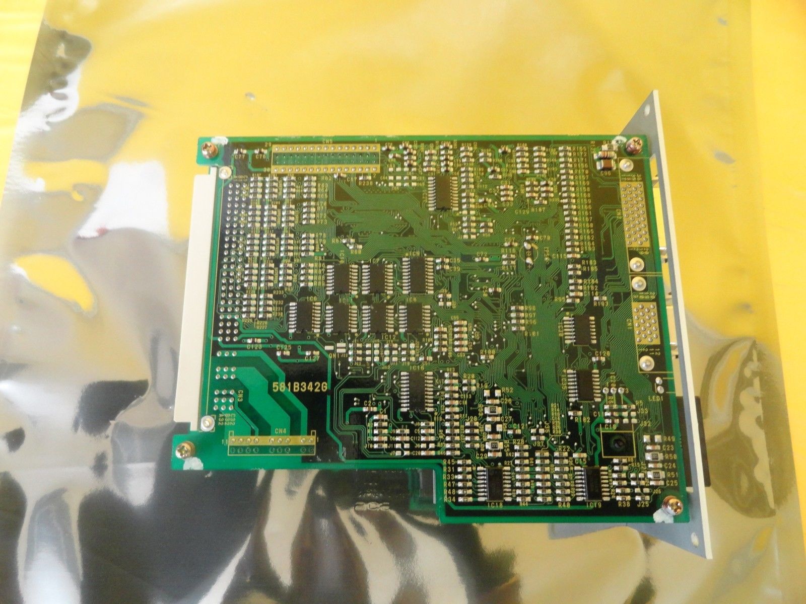
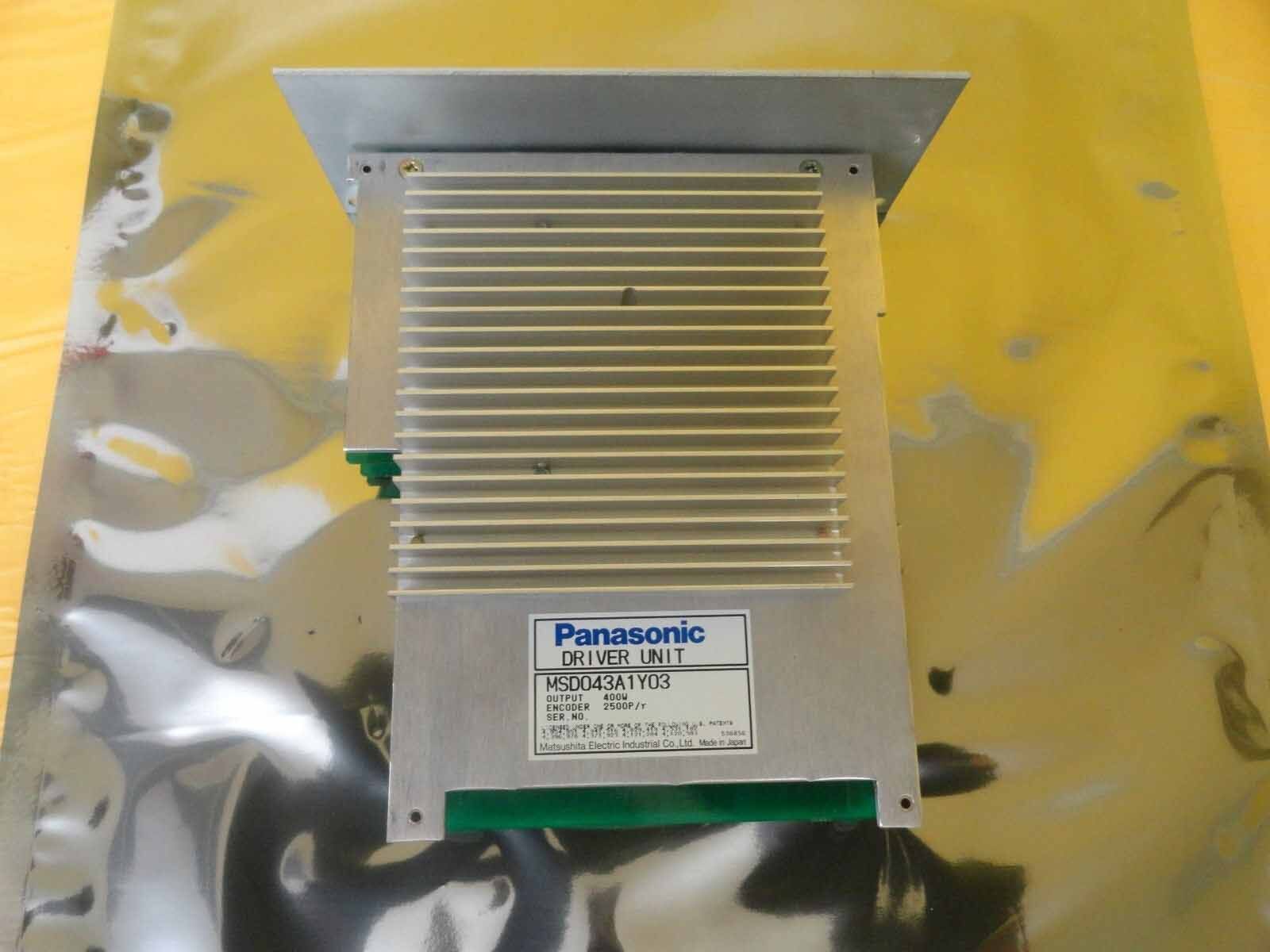
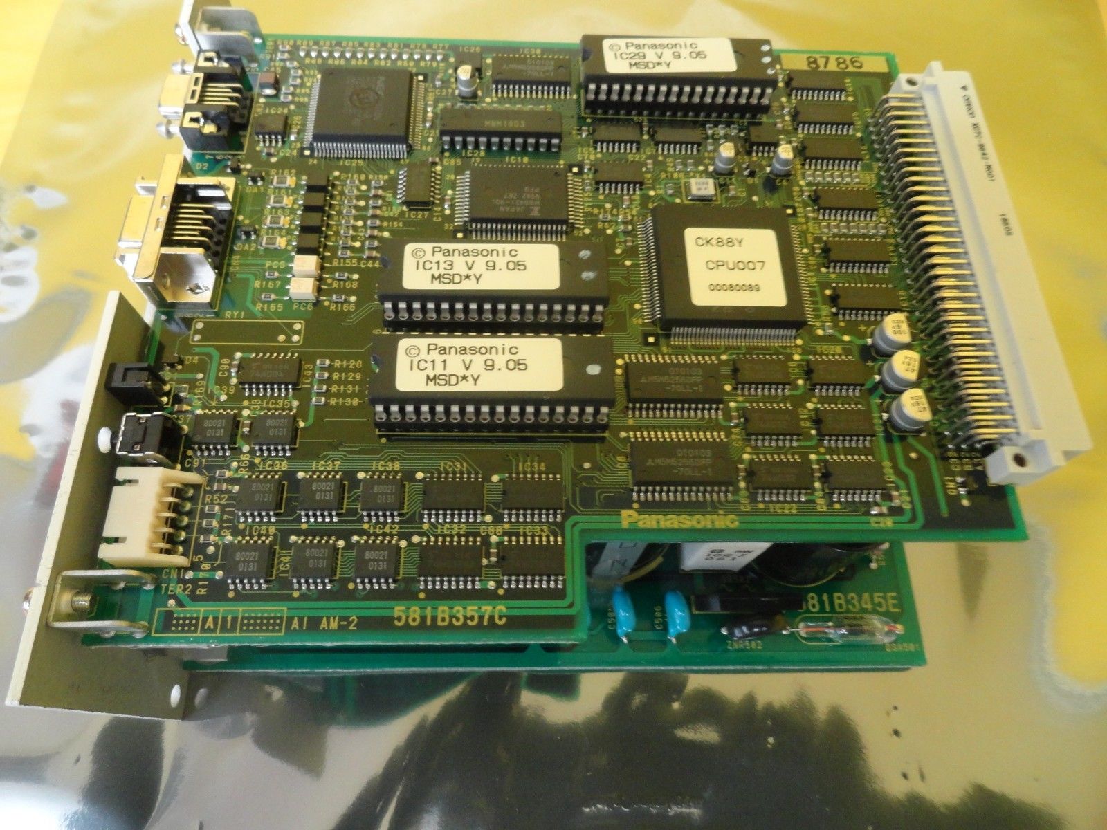
Driver control assembly, P/N: MSD261Y81
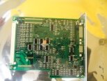
Installed PCB Cards:
Power Supply PCB, P/N: 581B345E
Communication PCB, P/N: 581B357C
Driver Unit PCB, P/N: MSD043A1Y03
X1 Driver Unit PCB, P/N: MSD3AZA1Y04
X2 Driver Unit PCB, P/N: MSD3AZA1Y04
X3 Driver Unit PCB, P/N: MSD3AZA1Y04.
TEL / TOKYO ELECTRON ACT 12 photoresist equipment is a lithography system used in the patterning process of advanced semiconductor device fabrication. It provides an advanced photoresist spin coating process to precisely apply thin film resists as well as high-precision exposure to pattern layers on advanced semiconductor chips. The unit is capable of spin coating up to four webs simultaneously with a spin speed of 7,000 rpm and a substrate temperature of up to 300°C. TEL ACT 12 can use photoresists with a wide range of exposure wavelengths, from UV to deep UV, and can provide up to 4500 wafer-datasets in one hour using the EBR mode. TOKYO ELECTRON ACT12 features a high-resolution zoom mapping machine which helps to match the resists used in the coat and expose process and helps to maintain uniform wafer thickness and high image quality across the entire surface of the wafer. This zoom mapping feature allows for very precise control of the resist thickness as a result of advanced spin coating position Regulation (SCPR). The SCPR tool enables a high level of accuracy to pre-set the photoresist positions on the wafer, ensuring a uniform film thickness uniformity during the spin coat process. ACT 12 photoresist asset is also equipped with advanced reactive ion etching (RIE), which can be used to etch very thin film layers on the wafer. RIE is a plasma-based etching process which allows for superior accuracy in patterning and control of surface features of advanced semiconductor wafers. It can be used to achieve extremely thin surface layers, pattern small features, and precisely control two- or three-dimensional features. RIEs can be used to produce epi-compatible structures (devices) with aspect ratios of 1:2 or higher with line widths of 0.35um. The model also features an advanced annotation capability with built-in software which provides the ability to precisely control the performance of the photoresist operations. It also allows for advanced annotation of patterns which can be used to fine tune the performance of the equipment. The system also features automatic aligner which helps in faster patterning and real-time defect inspection. TEL / TOKYO ELECTRON ACT12 photoresist unit is designed to meet the highest requirements of the manufacturing of advanced patterning processes for semiconductor devices. With its features, the machine is capable of providing high-precision coat and expose processes, high-resolution zoom mapping, fast RIE etching, and advanced annotation capabilities. This advanced tool helps ensure the production of high-performance, highly reliable devices.
There are no reviews yet

