Used TEL / TOKYO ELECTRON ACT 12 #9112122 for sale
URL successfully copied!
Tap to zoom













ID: 9112122
Wafer Size: 8"
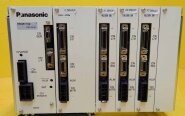
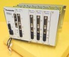
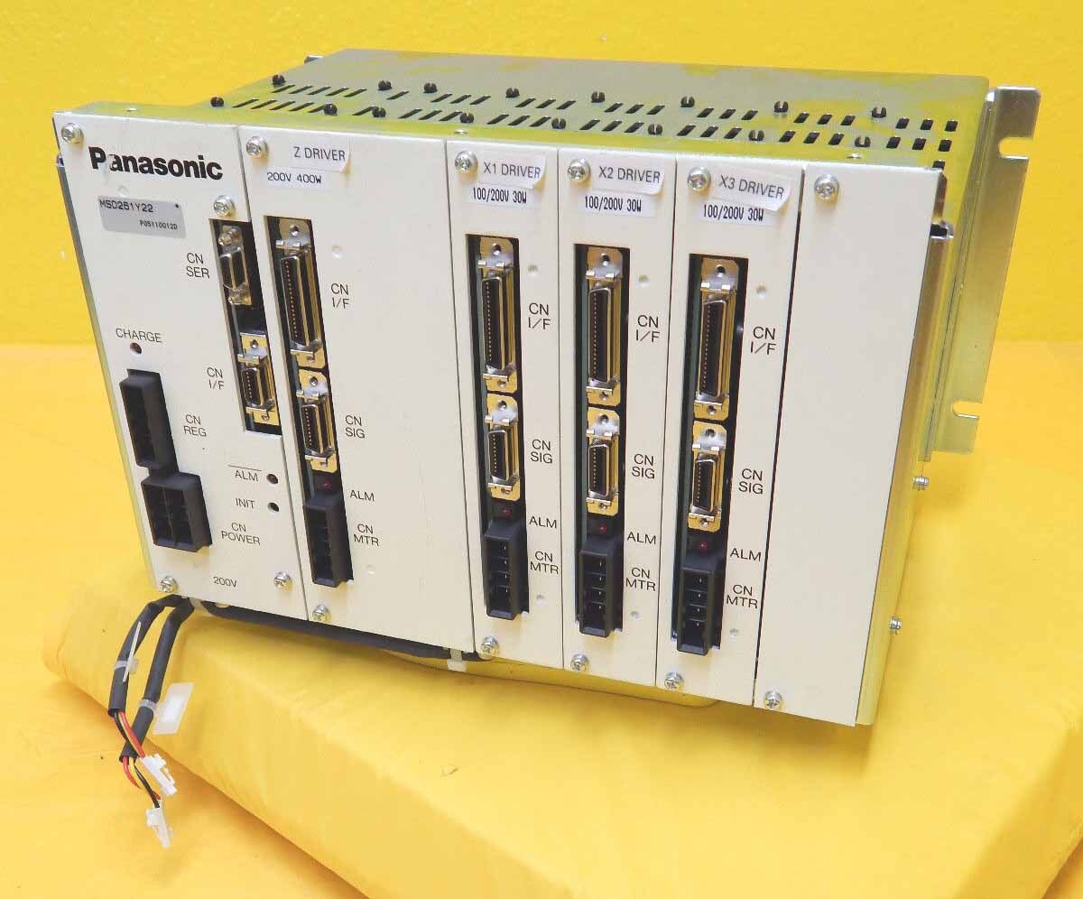
Driver Control Assembly, 8"
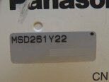
Panasonic, P/N: MSD261Y22
Installed PCB Cards:
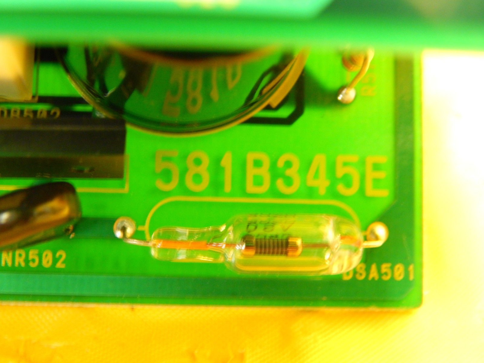
Power Supply PCB, P/N: 581B345E
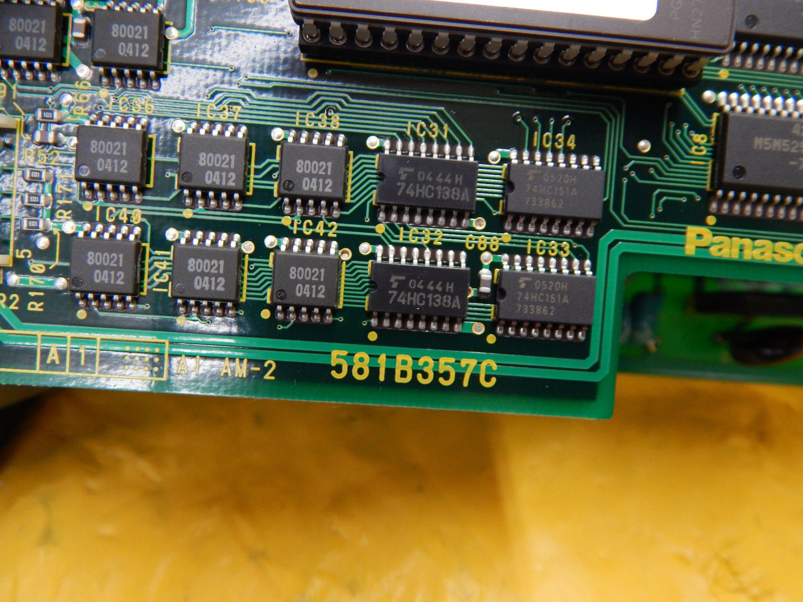
Communication PCB, P/N: 581B357C
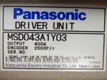
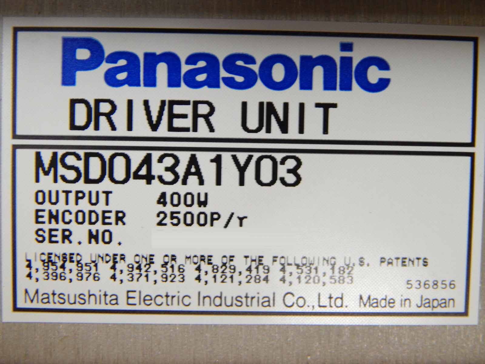
Z Driver Unit, P/N: MSD043A1Y03
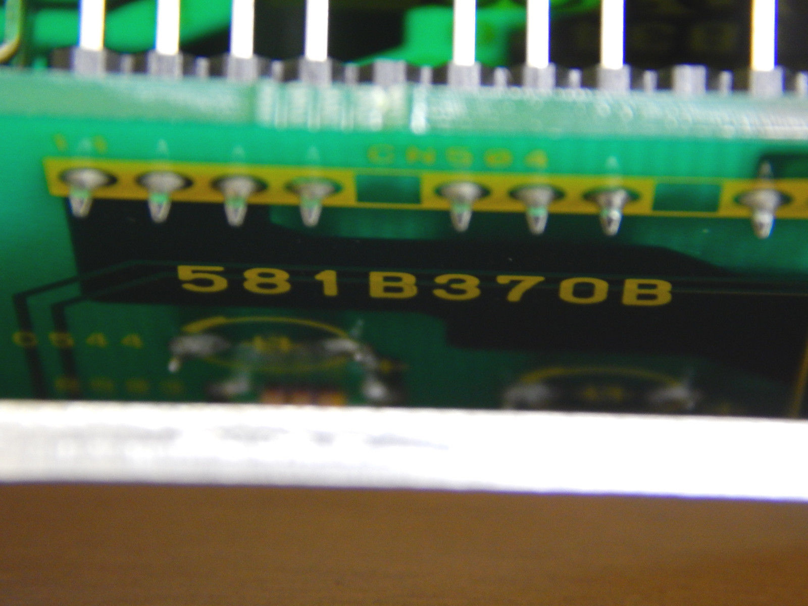
Z Driver Comm PCB, P/N: 581B370B
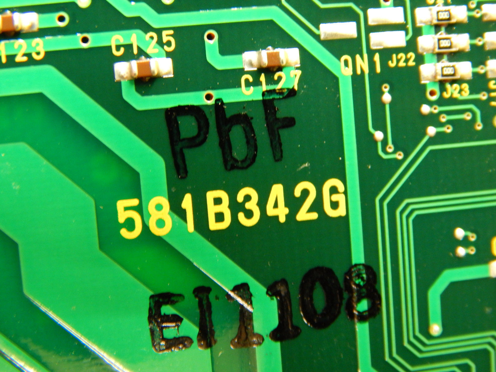
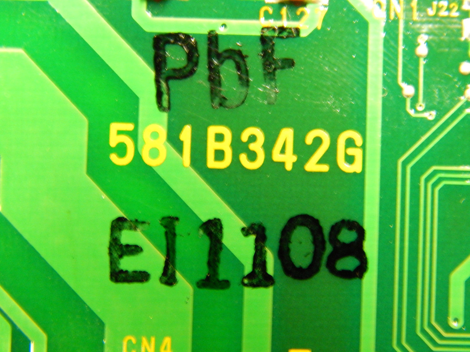
Z Driver I/O PCB, P/N: 581B342G
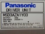
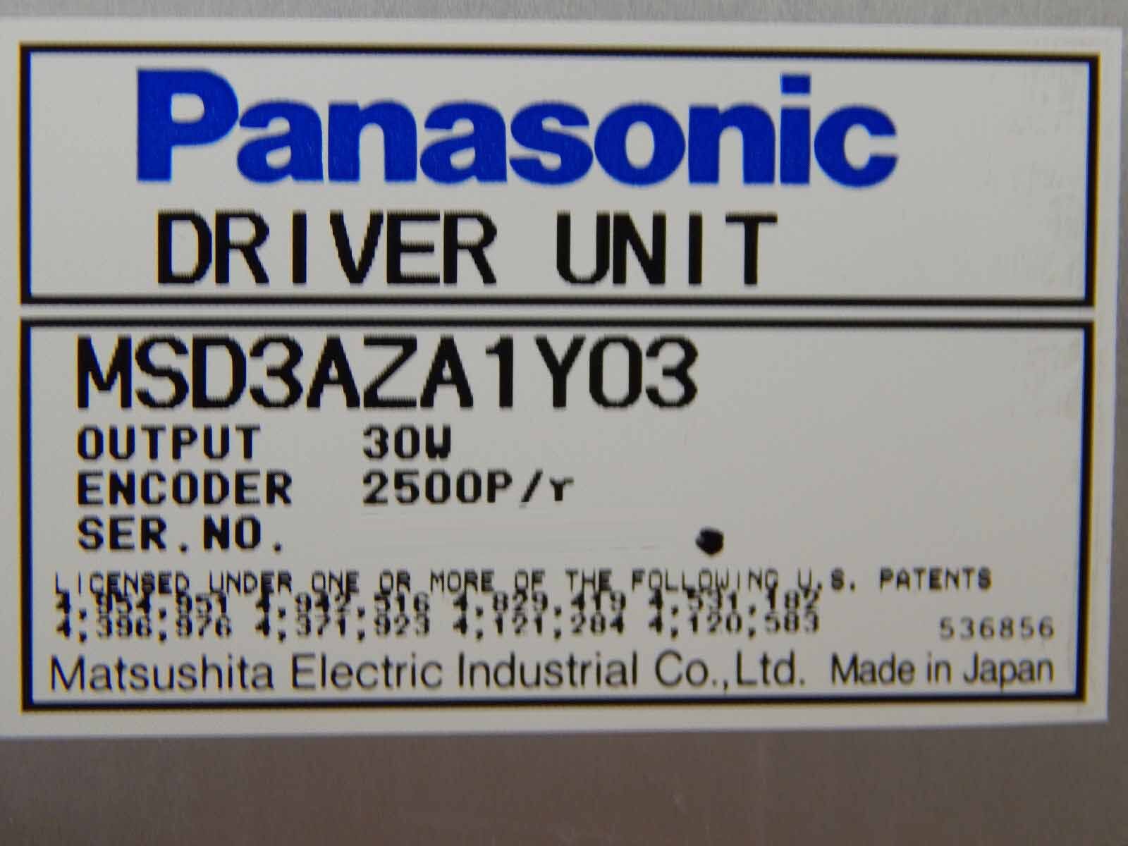
X Driver Unit, P/N: MSD3AZA1Y03
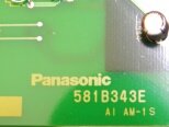
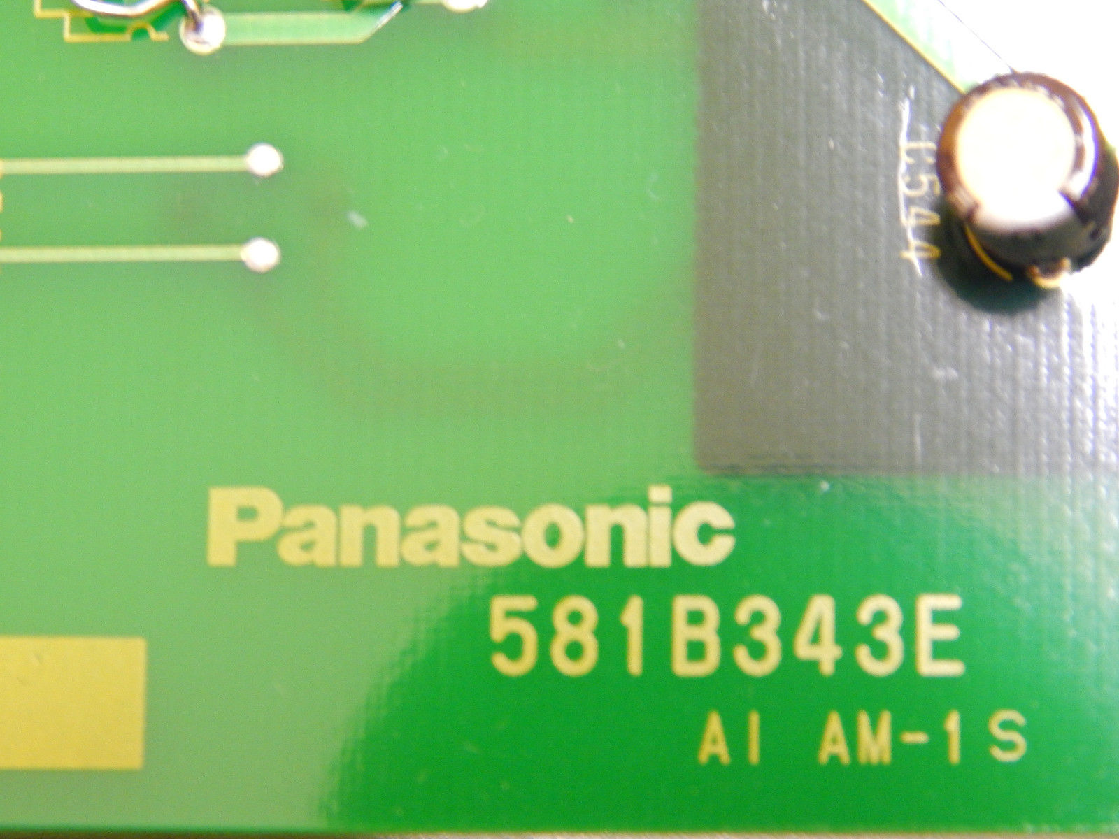
X Driver Comm PCB, P/N: 581B343E
Driver I/O PCB, P/N: 581B342G.
TEL / TOKYO ELECTRON ACT 12 is a photoresist equipment used for advanced semiconductor device fabrication processes. This system utilizes a high-speed, high-resolution maskless aligner to provide precise patterning of photoresists, antireflective layers, and other materials used for semiconductor device fabrication. At the heart of TEL ACT 12 is its high-speed, high-resolution maskless aligner. The aligner features an integrated spatial light modulator (SLM) combined with an objective lens to accurately pattern photoresist materials with an exposure resolution of 0.8 μm or greater. The SLM contains thousands of individually addressable reflective elements which can modulate the laser beam to quickly and accurately acquire images. The precise patterning of the photoresist allows submicron feature definition of complex multilayer structures. TOKYO ELECTRON ACT12 unit is also equipped with a wafer loader and temperature control to ensure uniform exposure of the photoresist layer. The wafer loader holds the wafer on a motorized conveyor belt and precisely positions it in the aligner machine. The temperature control uses an integrated cooling unit to ensure the photoresist is maintained at the correct temperature for exposure. ACT12 also features an automatic defect inspection tool which can detect defects in the photoresist layer such as pinholes, scratches, and voids. The tool's advanced processing algorithms analyze the photoresist layer and identify defects so that engineers can quickly and easily identify and address them before continuing with the device fabrication process. Finally, TOKYO ELECTRON ACT 12 asset is capable of handling a wide variety of photoresist materials used in semiconductor device fabrication. It is also compatible with a variety of exposure processes such as direct-write, step & repeat, and step & scan. The model can be used for a wide range of device applications, such as MEMS devices, and can be integrated with other systems such as electron beam lithography for further device complexity.
There are no reviews yet
