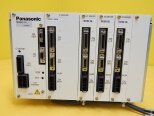
Used TEL / TOKYO ELECTRON ACT 12 #9112903 for sale
URL successfully copied!
Tap to zoom
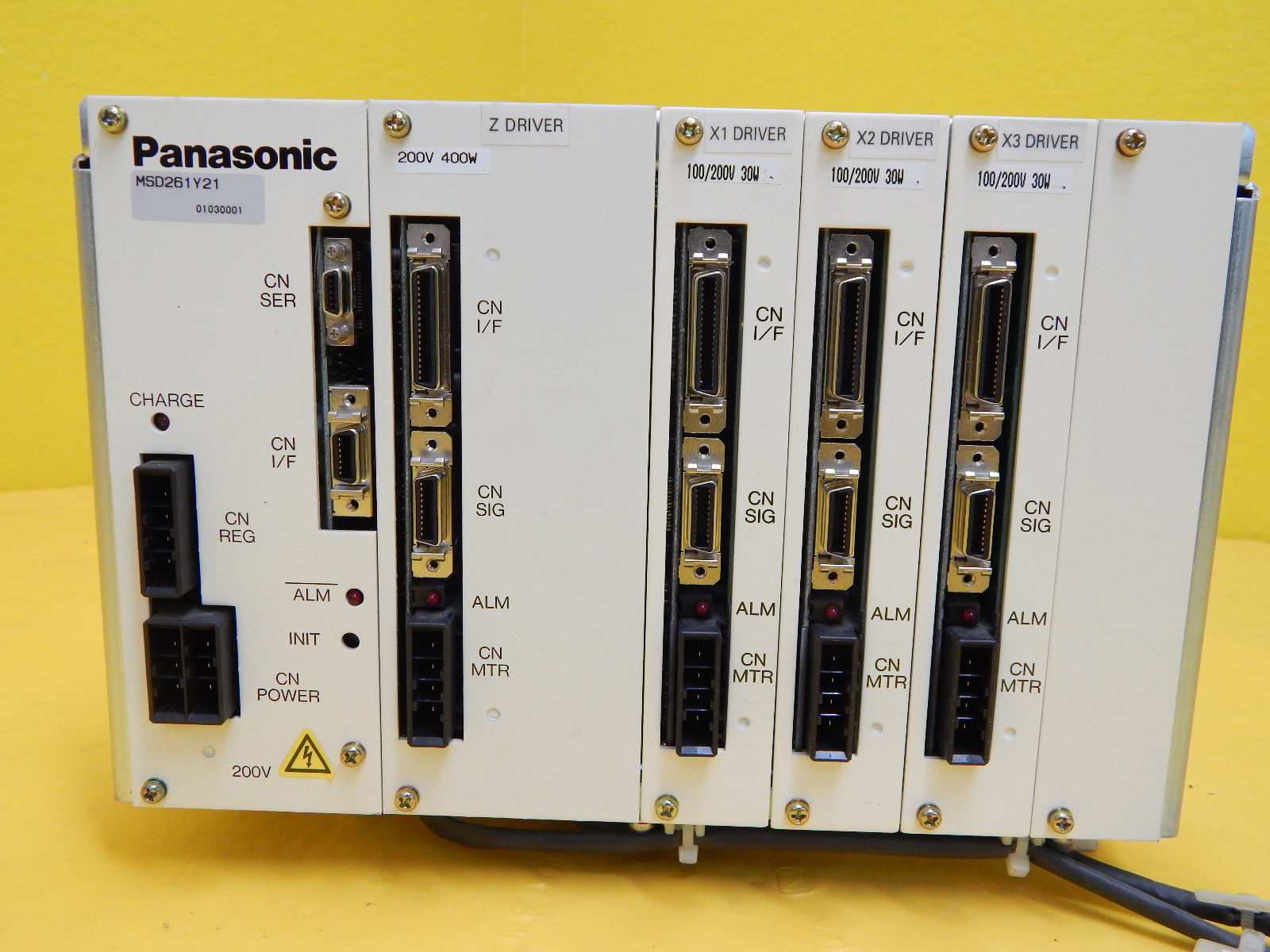












ID: 9112903
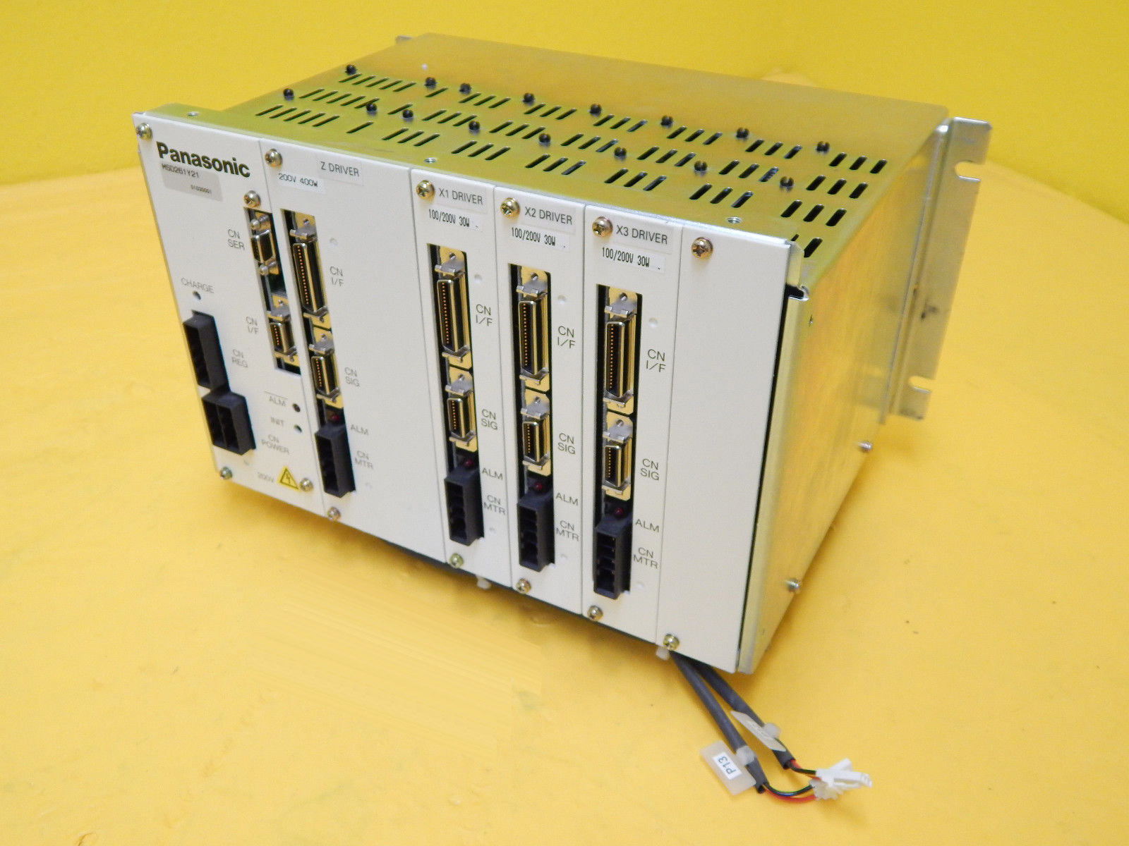
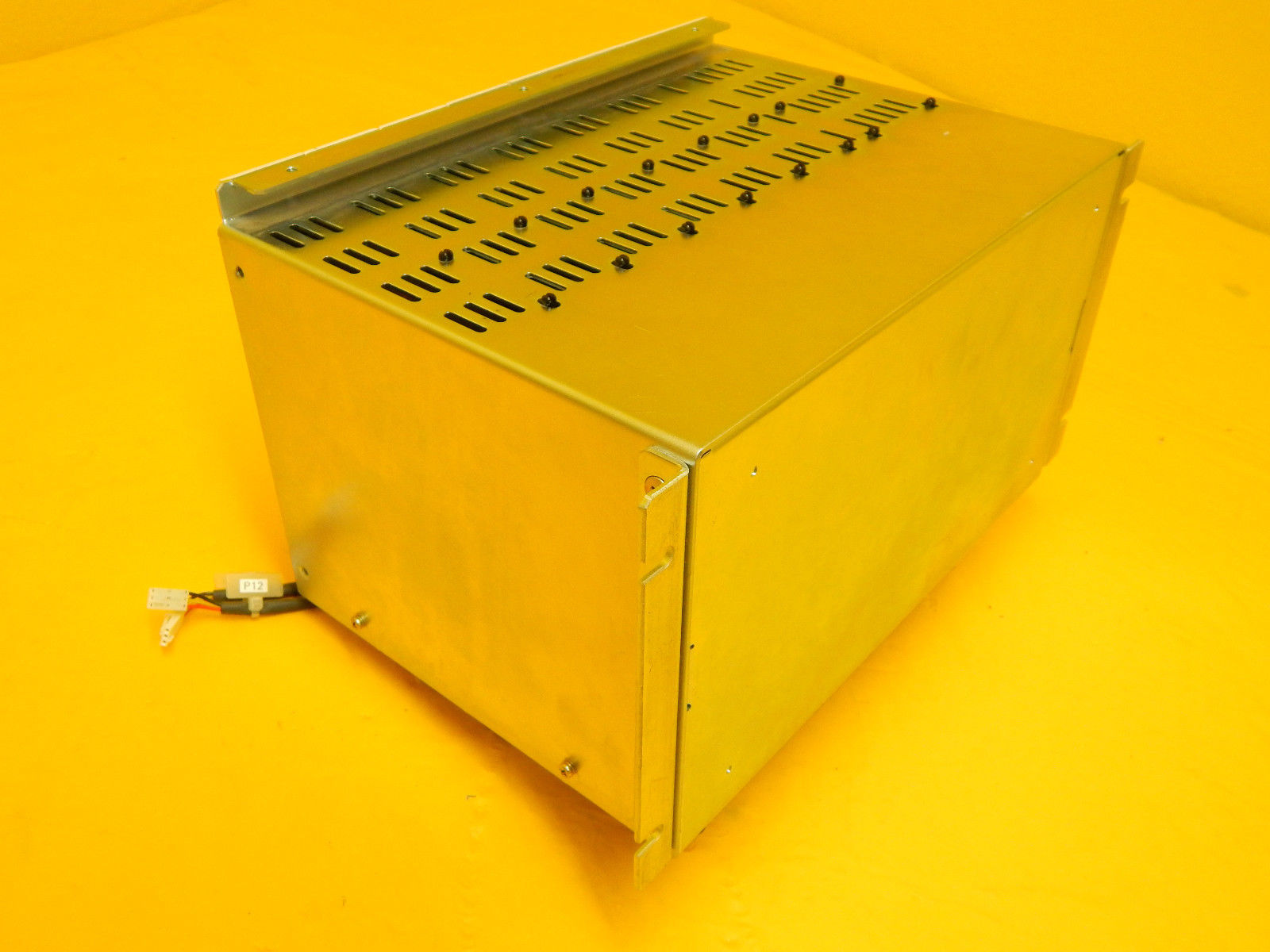
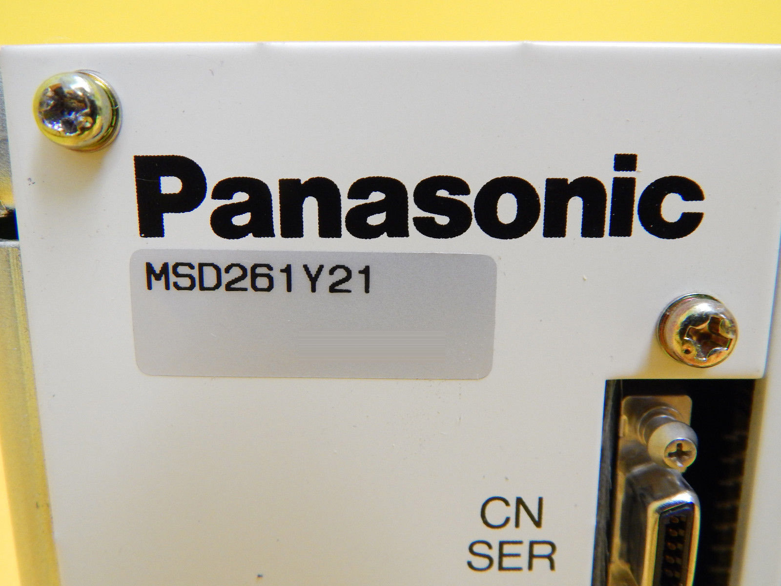
Driver Control Assembly, 8"
Panasonic, P/N: MSD261Y21
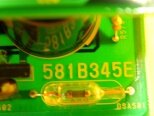
Power Supply PCB, P/N: 581B345E
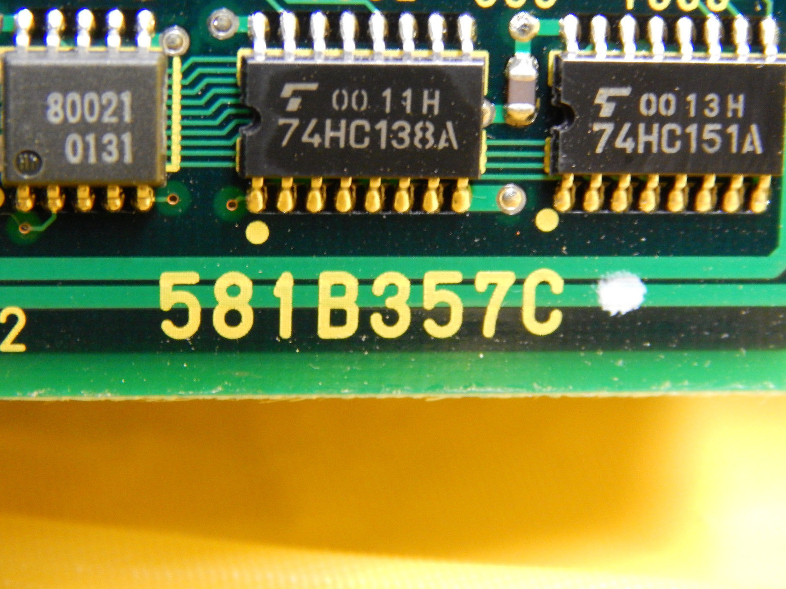
Communication PC, P/N: 581B357C
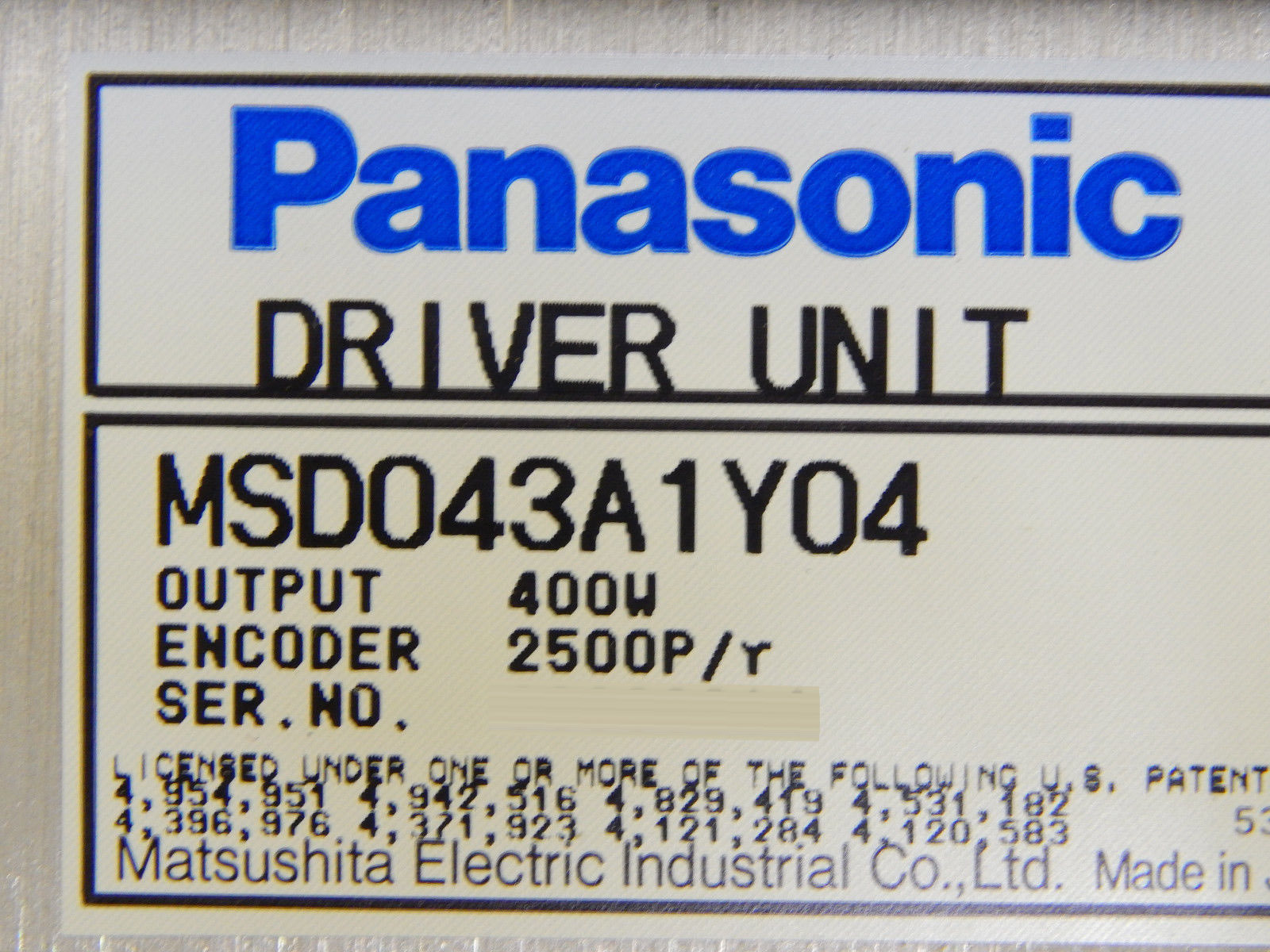
Z Driver Unit, P/N: MSD043A1Y04
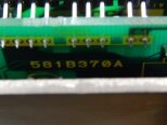
Z Driver Comm PCB, P/N: 581B370A
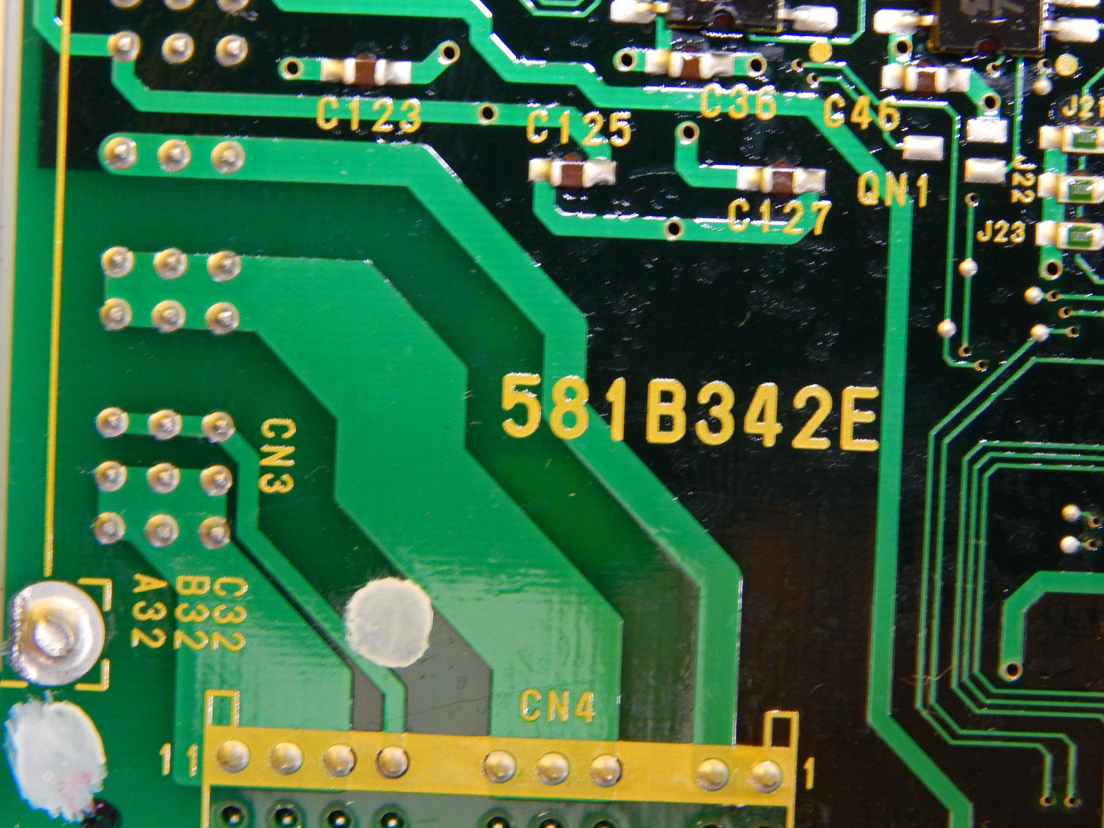
Z Driver I/O PCB, P/N: 581B342E
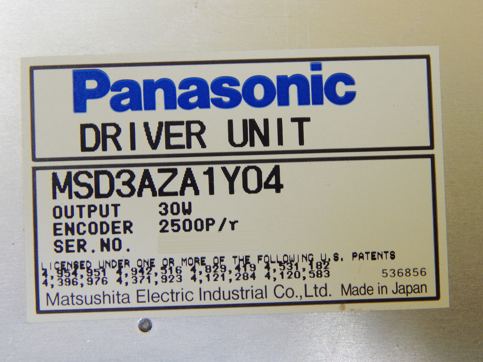
(3) X Driver Unit, P/N: MSD3AZA1Y04
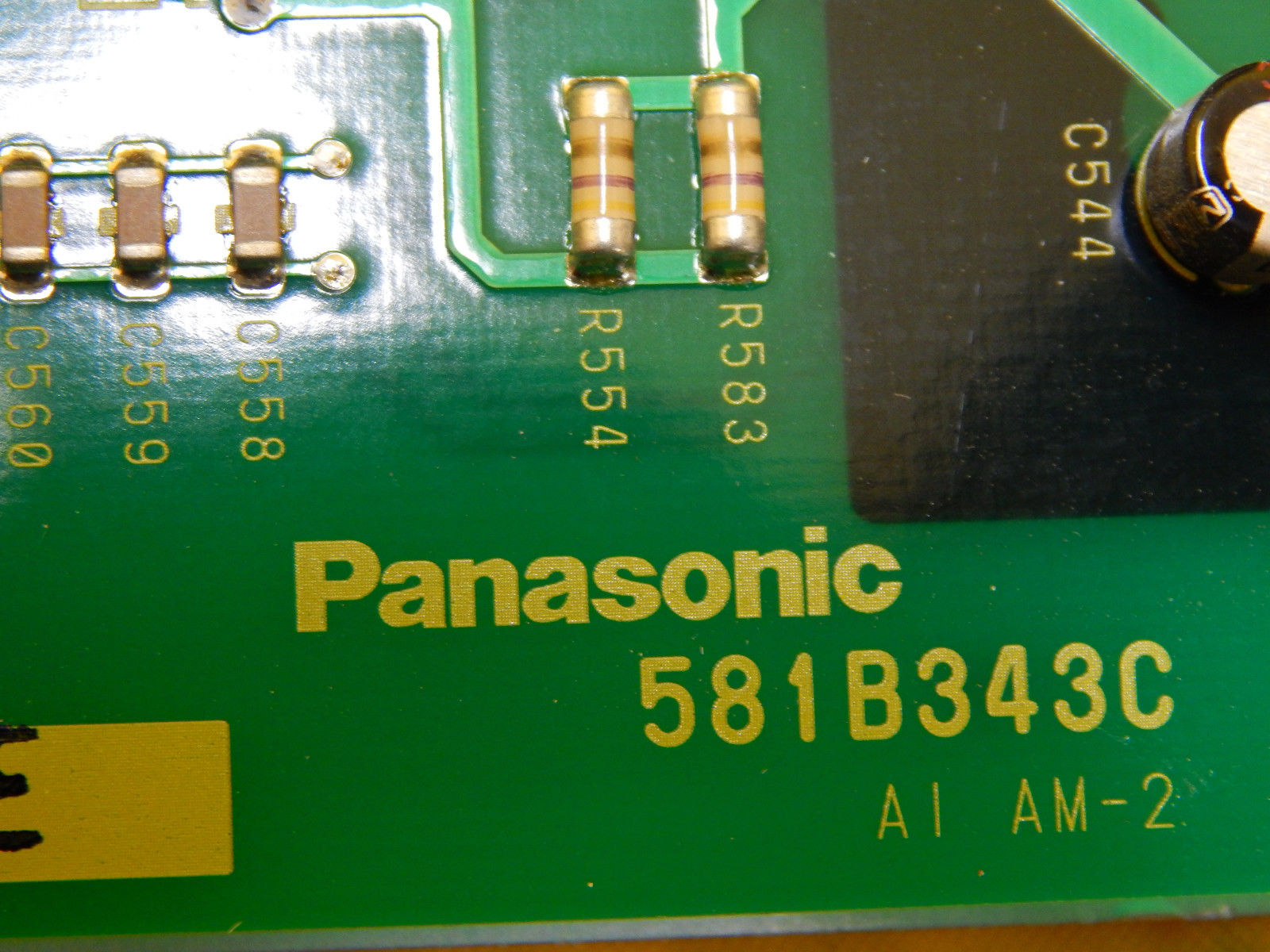
(3) X Driver Comm PCB, P/N: 581B343C
(3) Driver I/O PCB, P/N: 581B342E.
TEL / TOKYO ELECTRON ACT 12 is a photoresist equipment used for semiconductor manufacturing. Photoresist systems are used to apply a photo-sensitive coating onto semiconductor wafers. The goal of using such systems is to create patterns on the wafer to control its electrical and other properties. TEL ACT 12 is an optimized photoresist system specifically designed for advanced semiconductor fabrication. It is an advanced tool featuring a built-in projector, dual focus spots, and a basket-style unload/load station. Depending on customer requirements, the unit can be programmed to deliver patterned layers with sub-resolution features down to 0.35 µm. TOKYO ELECTRON ACT12 is equipped with a double-level 12-inch outer-cassette, which ensures that the wafers are firmly held during processing. The projection exposure machine delivers highly precise images over a wide exposure area. The projector is equipped with a laser-interferometer coupled with an auto-alignment tool that ensures accurate projection. The dual-focus spots, which are optimized based on a mathematical algorithm, also help enhance the accuracy of the projected image. In addition, the asset also features an integrated redundancy model. This ensures that, in case of a equipment fault, it fails safely and does not damage the wafers. The system also includes a low-vibration, top-of-the-range conveyor unit, which minimizes vibrations during processing, reducing damage to the wafers. Finally, ACT 12 is designed with a user-friendly graphical interface. This is intended to make machine setup and pattern creation easier and quicker. The tool is also outfitted with an embedded monitor module which continuously monitors the asset performance and provides detailed feedback of any abnormalities. Overall, TOKYO ELECTRON ACT 12 is a powerful photoresist model designed specifically for use in advanced semiconductor fabrication. Incorporating features such as auto-alignment, dual focus spots, and a equipment redundancy system, the unit provides high precision and reliability for creating complex patterns on semiconductor wafers.
There are no reviews yet
