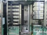
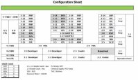
Used TEL / TOKYO ELECTRON ACT 12 #9163162 for sale
URL successfully copied!
Tap to zoom






ID: 9163162
Wafer Size: 12"
Vintage: 2007
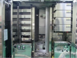
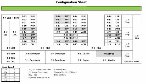
Coater / Developer system, 12"
2007 vintage.
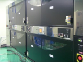
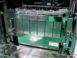
TEL / TOKYO ELECTRON ACT 12 photoresist equipment is a semi-automatic system developed for substrate processing. It is used in LED device fabrication processes such as mask patterning, contact hole formation, post-etch cleaning and others. It is mainly built for applications such as semiconductor device manufacturing, LCD panel manufacturing, micro film fabrication, medical device fabrication, and optics element manufacturing. TEL ACT 12 unit is designed to provide highly uniform photoresist coating on substrates such as glass, plastic, and metal. It is equipped with a high-speed process head that features precise coating technology as well as multi-row process accuracy. The machine also offers excellent performance of wet processing and pre-bake and post-exposure bake units. This tool features extremely flexible real-time process parameter adjustment systems with high precision temperature and atmosphere controls. The substrate is heated up to a specified temperature for precise resist coating on the wafer. The vacuum chuck is used to hold the wafer flush with the coating optics. This measures the coating variation so that the coating film can be maintained uniform. The coating fluid is then applied from a spinning coater and is dried by a high-speed spin-off wheel to uniform thin film thickness. The asset can apply the photoresist with high precision and uniformity for a variety of wafer diameters and thickness up to 80mm. A post exposure bake process follows the photo masking process to promote good adhesion of the resist film to the wafer and also minimize resist distortion during development and etching. The photoresist is optically designed to provide higher sensitivity with low background exposure dose for the photolithography processes. The wafer is exposed through the photo mask with TOKYO ELECTRON ACT12 model to expose the desired features. This occurs in microsecond time frames for short exposure duration and high-resolution patterning. The photoresist is then developed in a developer to expose the non-compatible parts of the wafer followed by etching. The developed parts are then removed by a spin-off wheel. The resist is then normally stripped using plasma, wet chemical, or laser removal methods for accurate patterning. TEL ACT12 photoresist equipment offers excellent photolithography and processing uniformity, which leads to improved yield in fabricating the LED devices. This system also offers flexibility and precise control in the wafer patterning processes, making it an ideal solution for the fabrication of various types of devices.
There are no reviews yet
