Used TEL / TOKYO ELECTRON ACT 12 #9164503 for sale
URL successfully copied!
Tap to zoom


ID: 9164503
Wafer Size: 8"
Vintage: 2001
DUV coater / developer, 8"
Dual block track for S204
Utilized with Nikon S204 Scanner Exposure Tool
iUSC SECSI, SECSII, HSMS, & GEM Interface Compatibility
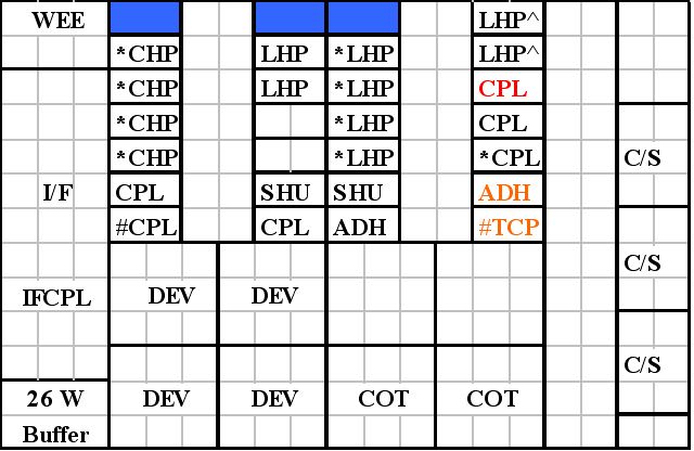
4 Blocks Interfaced: Cassette-2 Process Blocks-Scanner Interface
4 Wafer Transfer Robot Arms: Cassette-2 Process Blocks-Scanner Interface
Control Module on Cassette End-Station (CES)
Interface Block:
Single-pincette shared wafer transfer with centering guides
Standard wafer arm and interface panel to accommodate stepper/scanner
Interface includes a CPL for insuring consistent wafer temps into the stepper/scanner
2 Coaters (COT):
4 resist nozzles with temperature control
16 layer resist and solvent filters
RRC Pumps
4L or 1L Nowpak capability
SS 0.3mm diameter side rinse nozzle with flow meter
2 SS 0.3mm diameter back rinse nozzles
4 Developers (DEV):
2 “H” nozzles with temperature control per cup
16 layer developer filter
Bulk-FSI system for developer
2 Adhesion Process Stations (ADH):
Half sealed chamber with dispersion plate for HMDS
6 Chill Plate Process Stations with temperature control (CPL)
1 Transfer Chill Plate (TCP)
8 Low Temperature Hot Plate Process Stations with temperature control (LHP)
4 Chilling Hot Plate Process Stations (CHP)
1 Wafer Edge Exposure Process Station (WEE)
DUV illumination monitor on lamp housing
Uses a 250W ultra pressure Mercury lamp with 5x4mm illumination pattern
Subcomponents:
Fluid Temperature Controller
Temperature & Humidity Controller - 2x
Chemical Cabinet
AC Power Box
2001 vintage.
TEL / TOKYO ELECTRON ACT 12 is a photoresist equipment that is used for two-dimensional photolithographic circuit patterning. The photoresist system includes a light source, optics, and a reticle, which masks off or blocks certain areas of a wafer in the production of integrated circuits. The light source used for TEL ACT 12 is a broad spectrum of ultraviolet (UV) light that is passed through the optics and then onto the reticle, where the circuit patterns are formed. The UV light interacts with the chemical coating layer on the wafer, which is then used in the production of different types of integrated circuits. The optics component is composed of several mirrors, lenses, and apertures. The mirrors guide the light beam into the reticle and onto the wafer, and the lenses control the convergence and divergence of the beam. The apertures control the size and shape of the beam, as well as the amount of light that is transmitted. The reticle is the core component of the photoresist unit and is used to mask off certain parts of the wafer from the light source. It is designed in such a way that it can efficiently expose certain areas of the wafer while blocking other areas. Once the wafer is exposed to the light source, certain areas on the wafer are etched away, resulting in the desired circuit pattern. TOKYO ELECTRON ACT12 photoresist machine is a key component in the production of integrated circuits. It provides a reliable and efficient method of patterning the wafer to the desired design, resulting in high quality and reliable components and circuits. The tool can be used for a variety of circuit designs with a high degree of accuracy, allowing for precise and repeatable results during the production of integrated circuits.
There are no reviews yet