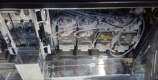
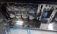
Used TEL / TOKYO ELECTRON ACT 12 #9237246 for sale
URL successfully copied!
Tap to zoom
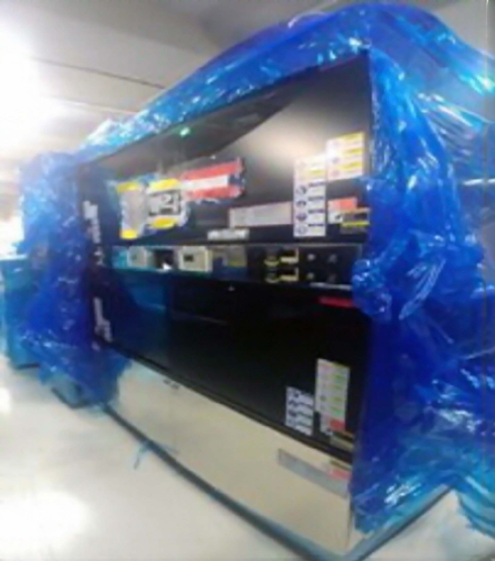


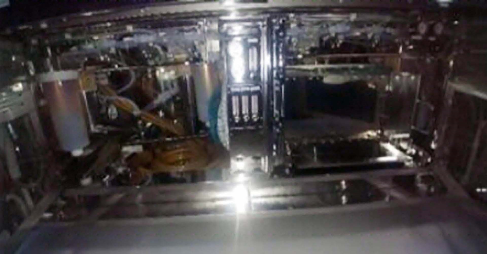

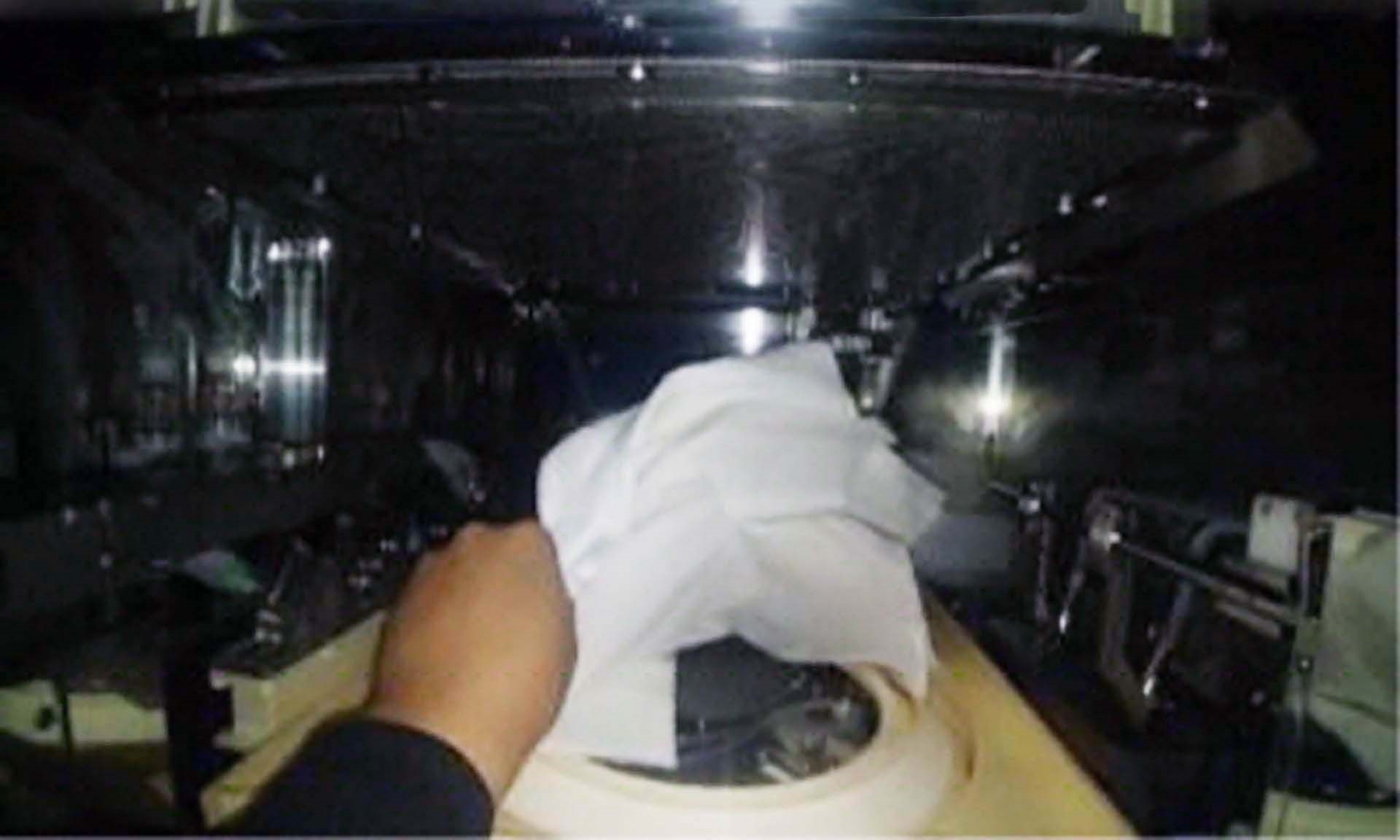


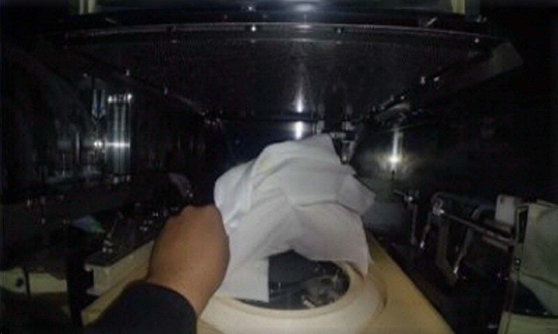

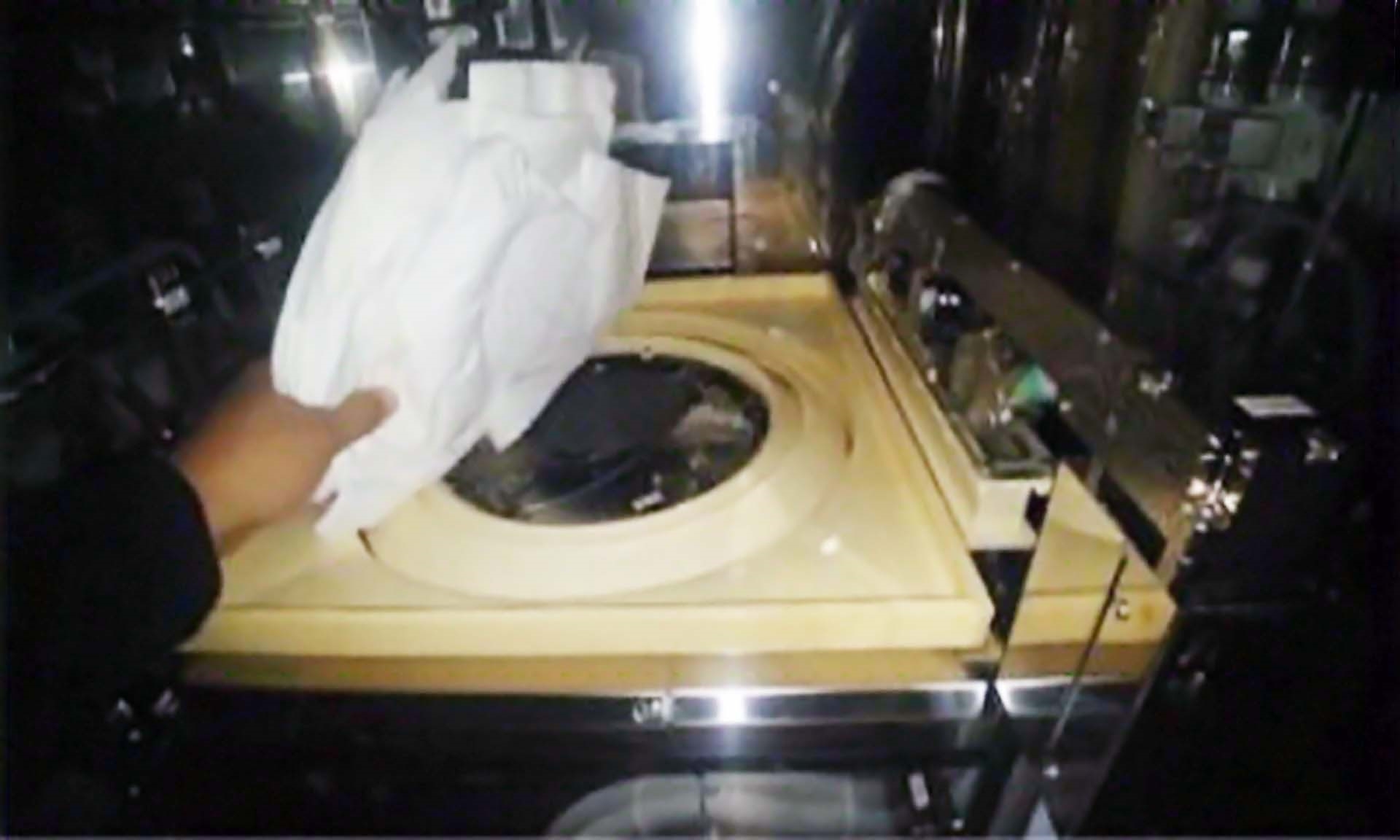

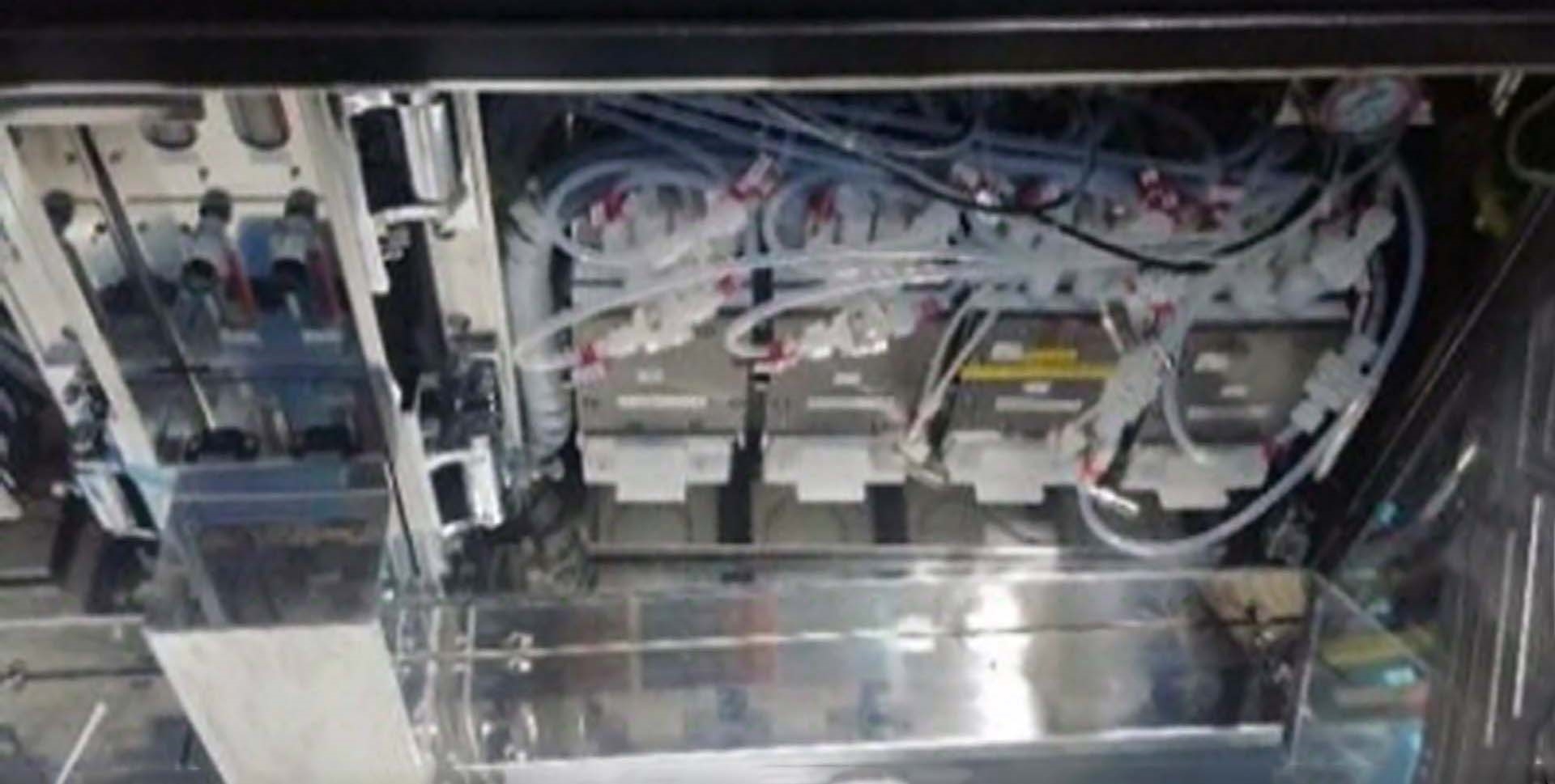

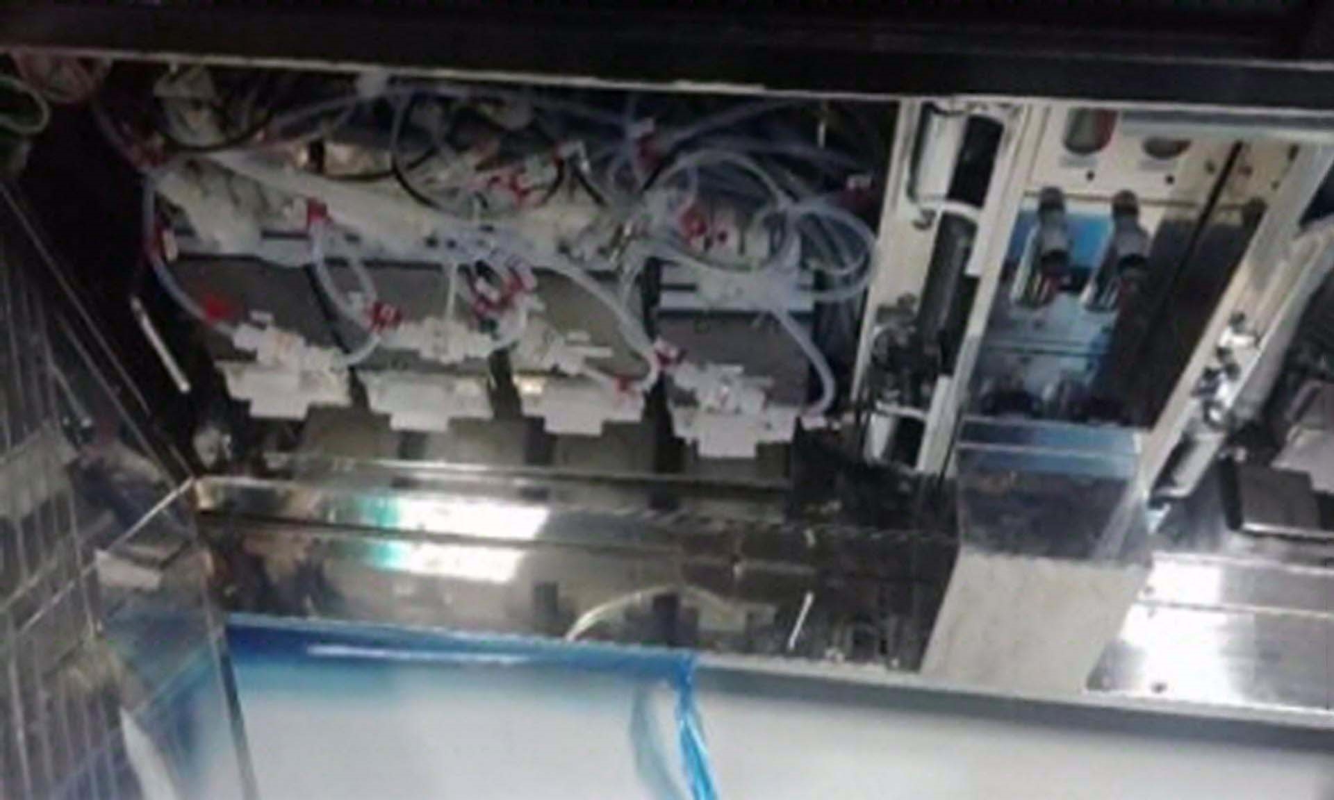


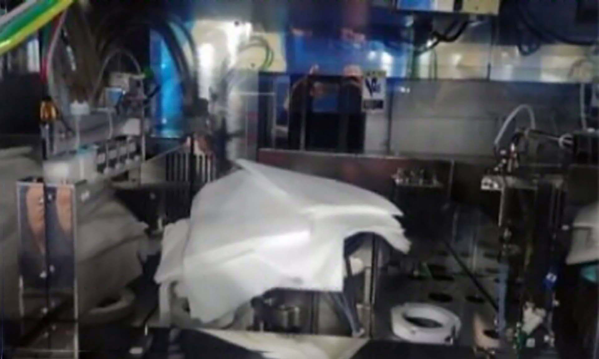

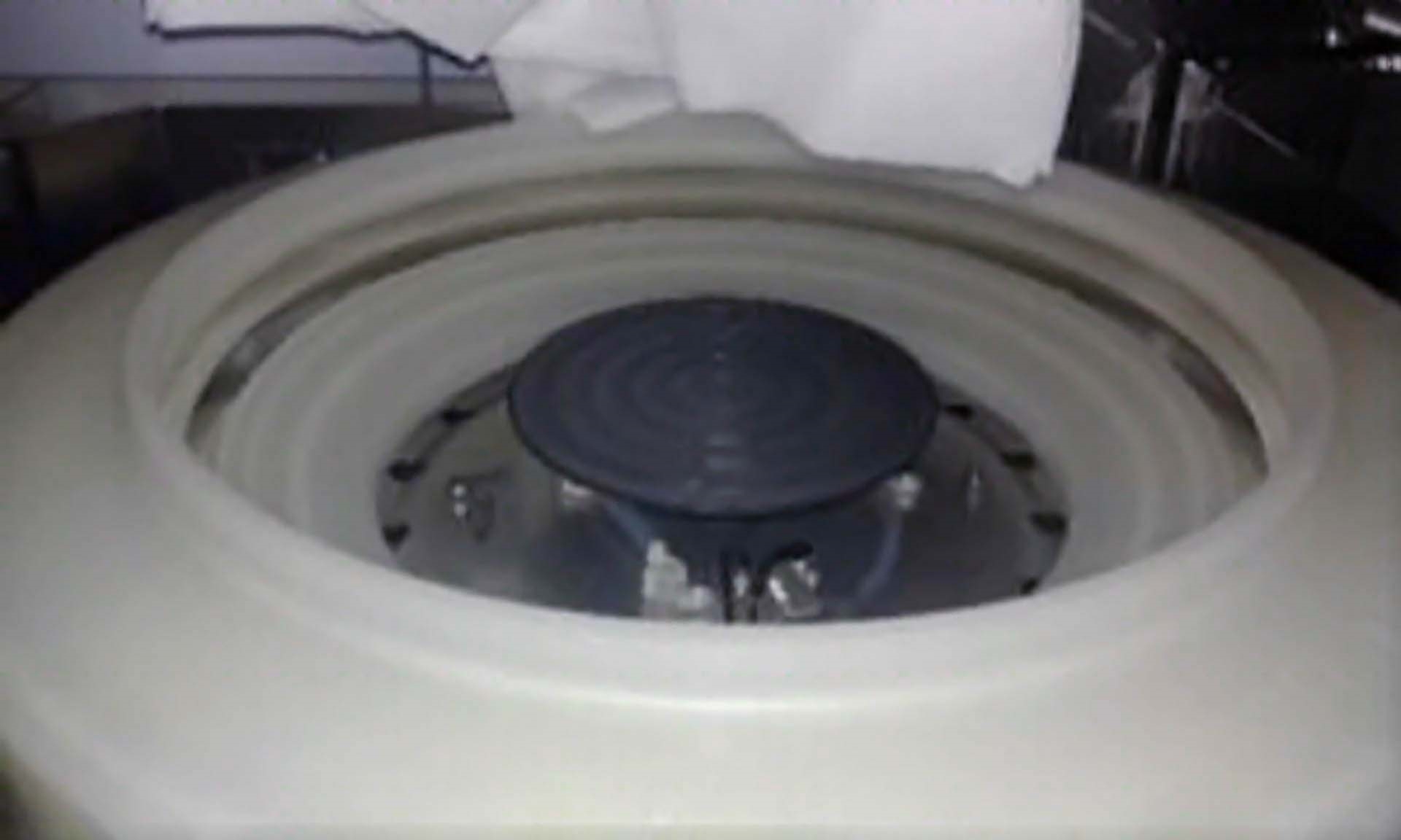


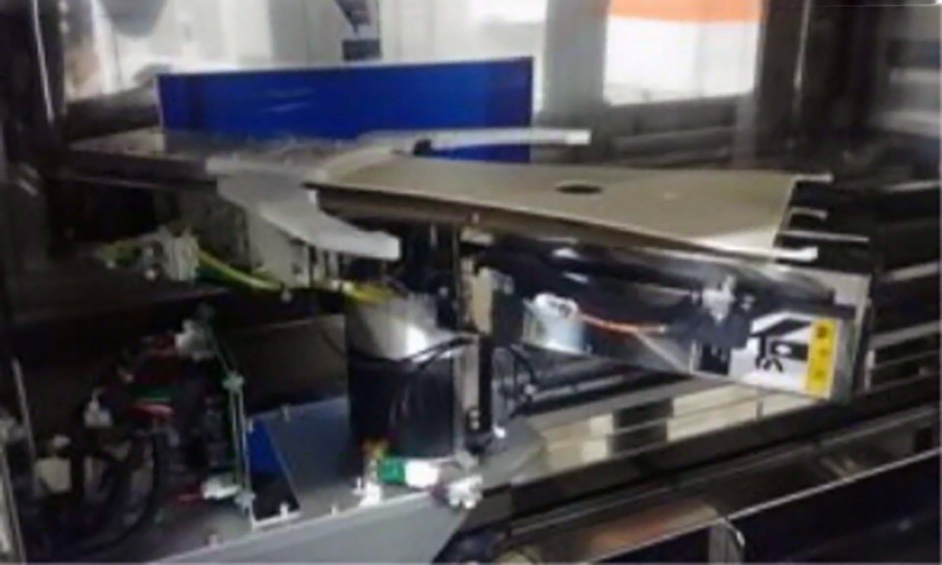





TEL / TOKYO ELECTRON ACT 12 is a photoresist equipment that utilizes an imaging and patterning technique for the purpose of creating nanoscale structures. The system utilizes beamprojecting optics, which are capable of projecting a focused beam of light that is roughly 0.1 micrometer in width onto a semiconductor wafer. This light is used to etch patterns into the photoresist material, which will form the structures at the nanoscale level. TEL ACT 12 offers a combination of a short focal range and a high optical numerical aperture. The unit also employs a patent-pending laser light imaging process for patterning at the nanoscale. This process uses a laser beam that is highly focused and has extremely low divergence, thus allowing for exceptional resolution on a nanometer scale. The machine also offers an advanced control tool with advanced editing tools for pattern optimization, which greatly enhances semiconductor device production. The platform provides pattern optimization with a high degree of precision, allowing nanoscale structures to be built to the exact specifications of the chip. TOKYO ELECTRON ACT12 also features a highly advanced substrate alignment asset, which provides a high level of accuracy for the controlled placement of the photoresist structures. This allows for precise placement of the structures and components on the wafer, and also reduces errors of the alignment or aberration of the nanoscale structures. The model also features an advanced imaging equipment. The optical system used in TEL / TOKYO ELECTRON ACT12 is capable of projecting images at a resolution of 15 nanometers, which allows for monitoring of the nanoscale structure fabrication process. Finally, TEL ACT12 offers a highly reliable and repeatable workflow process. The unit is powered by the highly-reliable Terapro Engine, which is capable of controlling the entire workflow process. The Terapro engine provides an accurate and reliable sequence of events for each imaging step, thus ensuring a consistent and reliable imaging process and thus reducing errors in the production process.
There are no reviews yet

