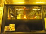
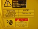
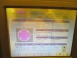
Used TEL / TOKYO ELECTRON ACT 12 #9255021 for sale
URL successfully copied!
Tap to zoom
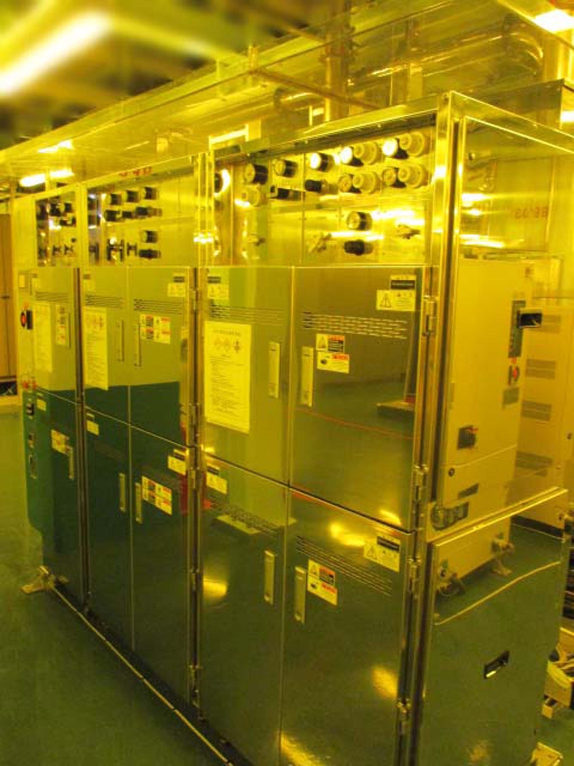

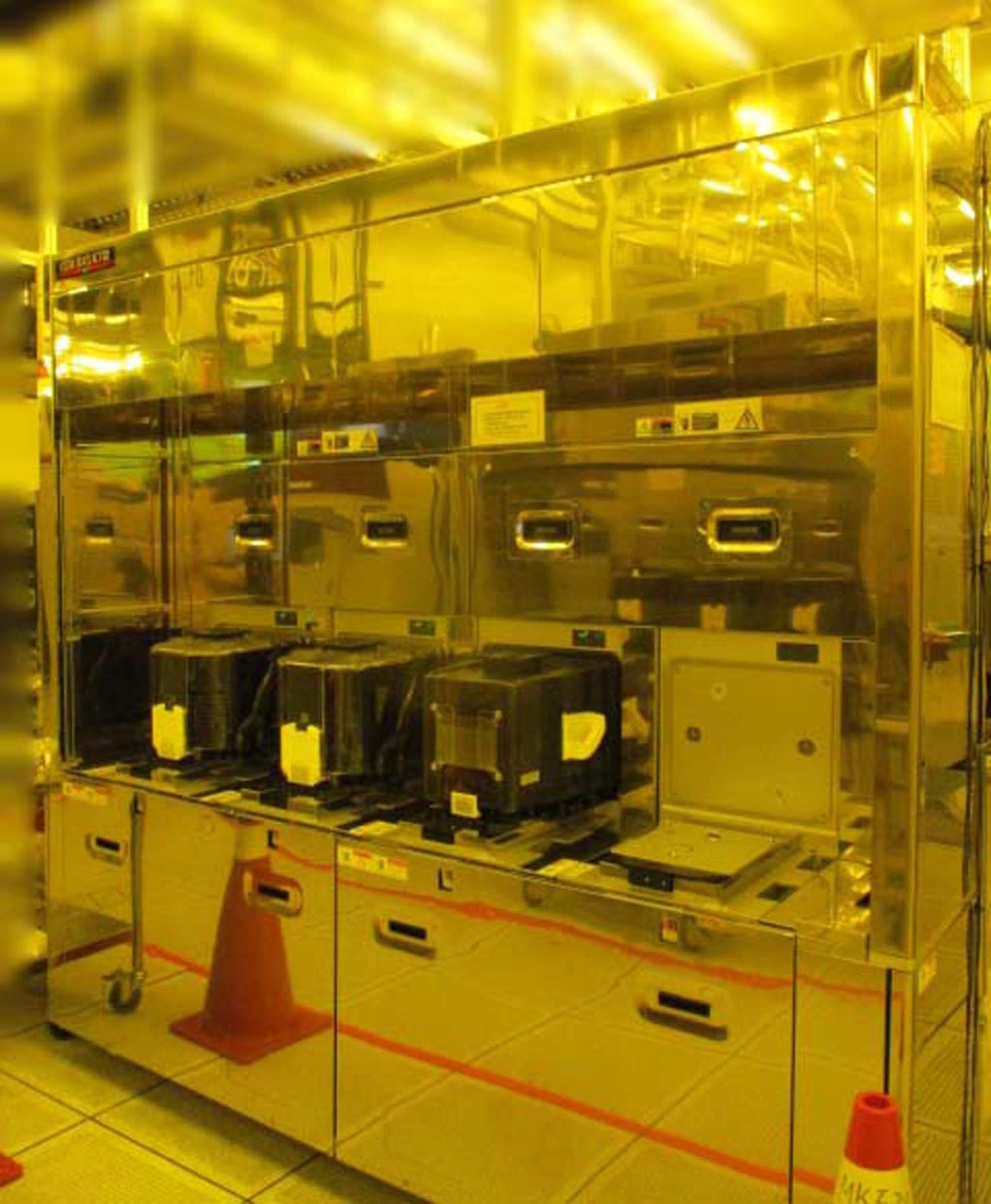

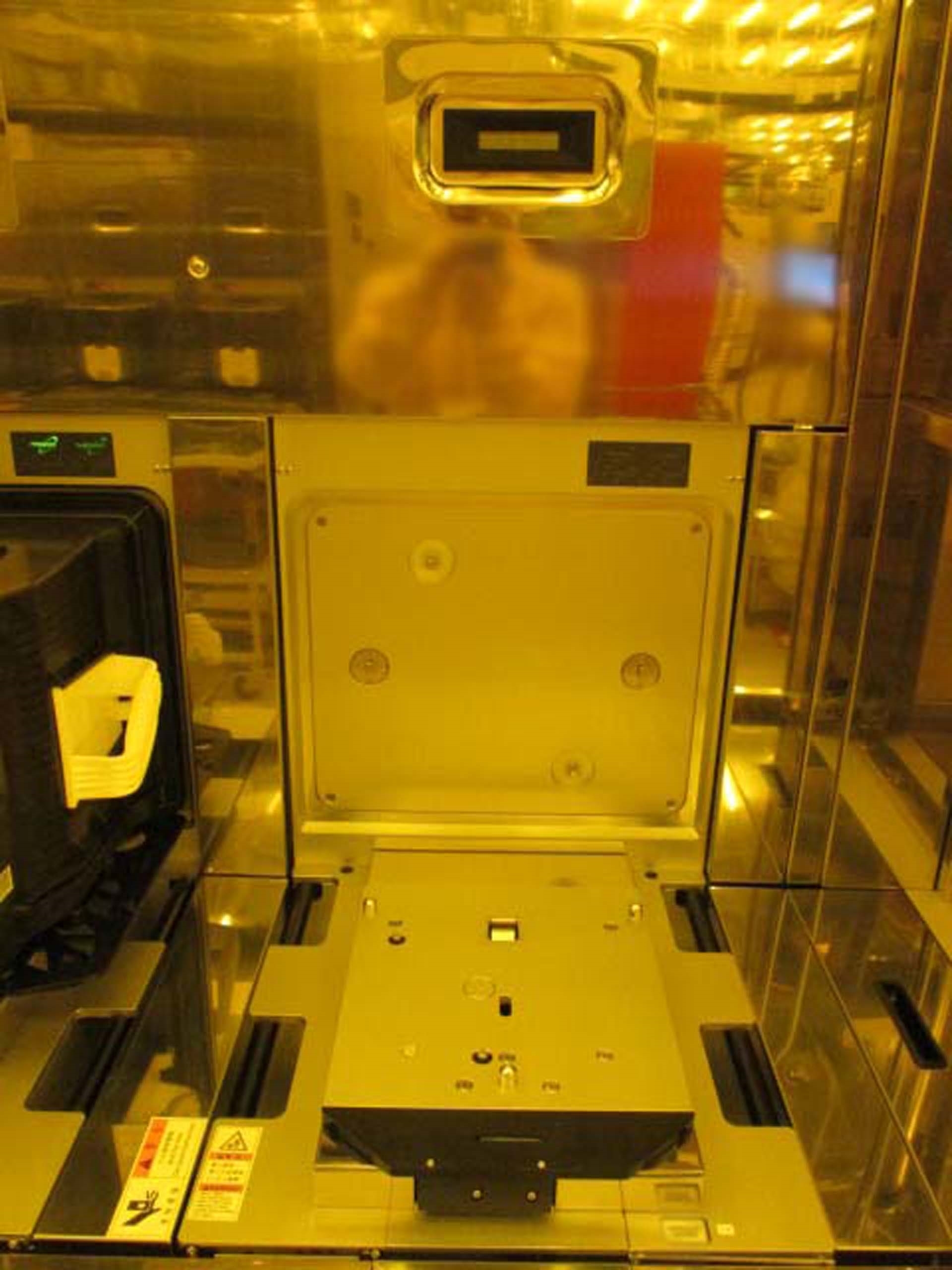

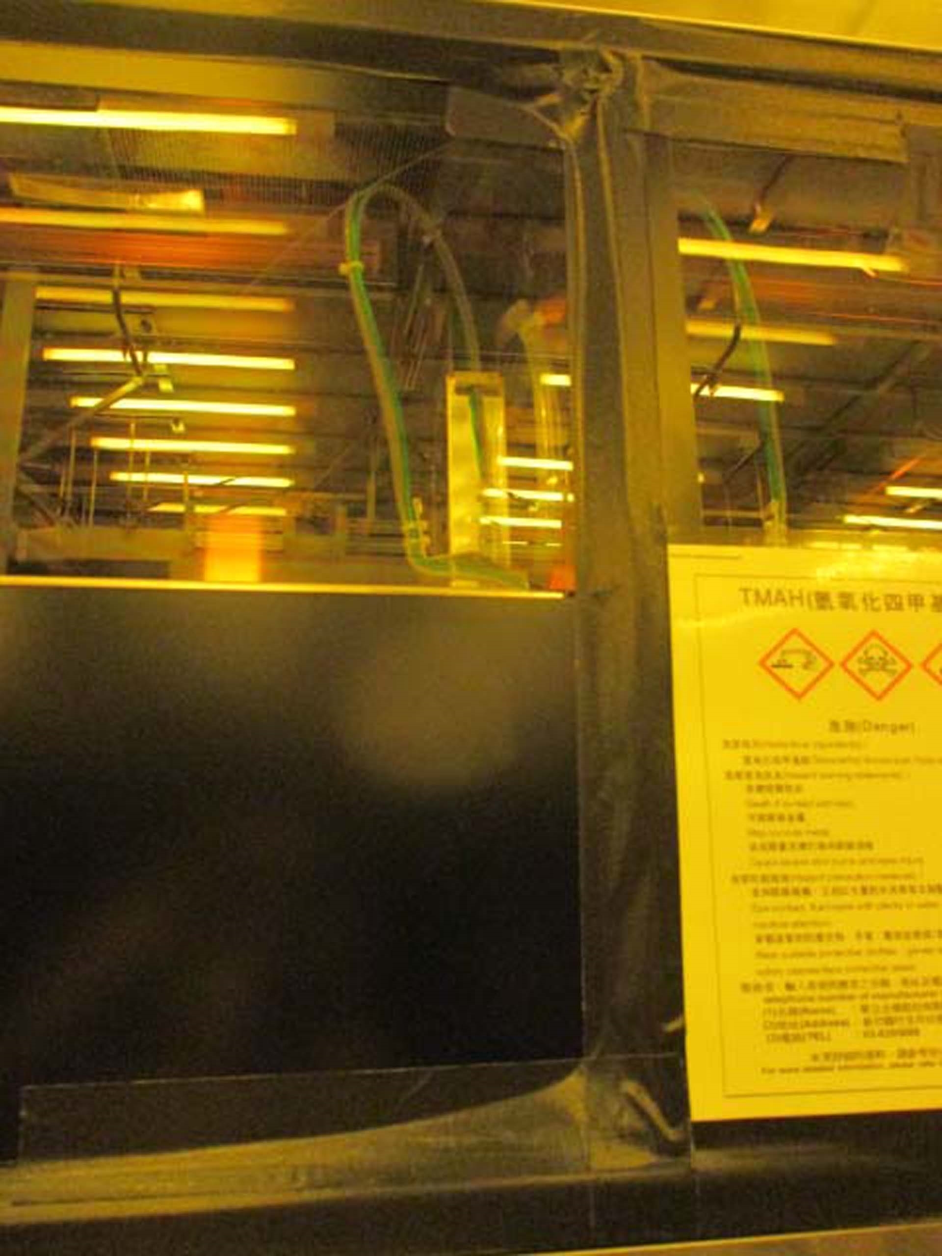

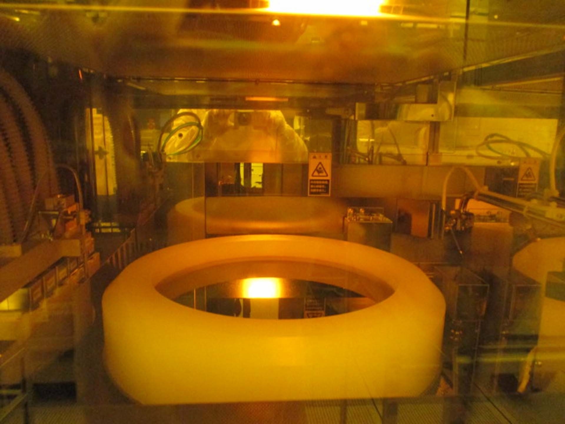

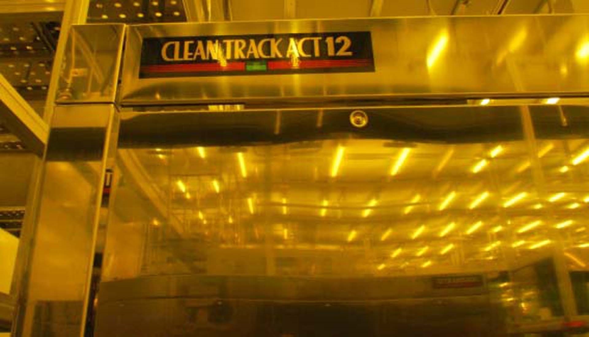

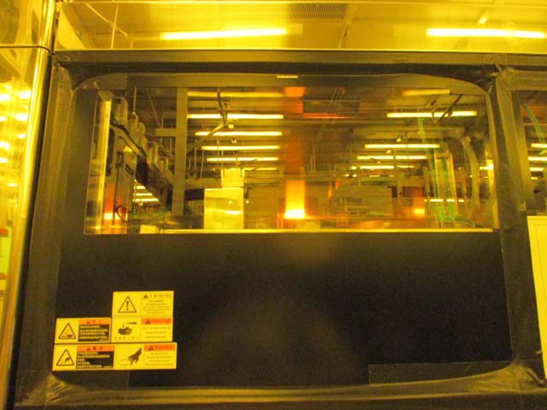






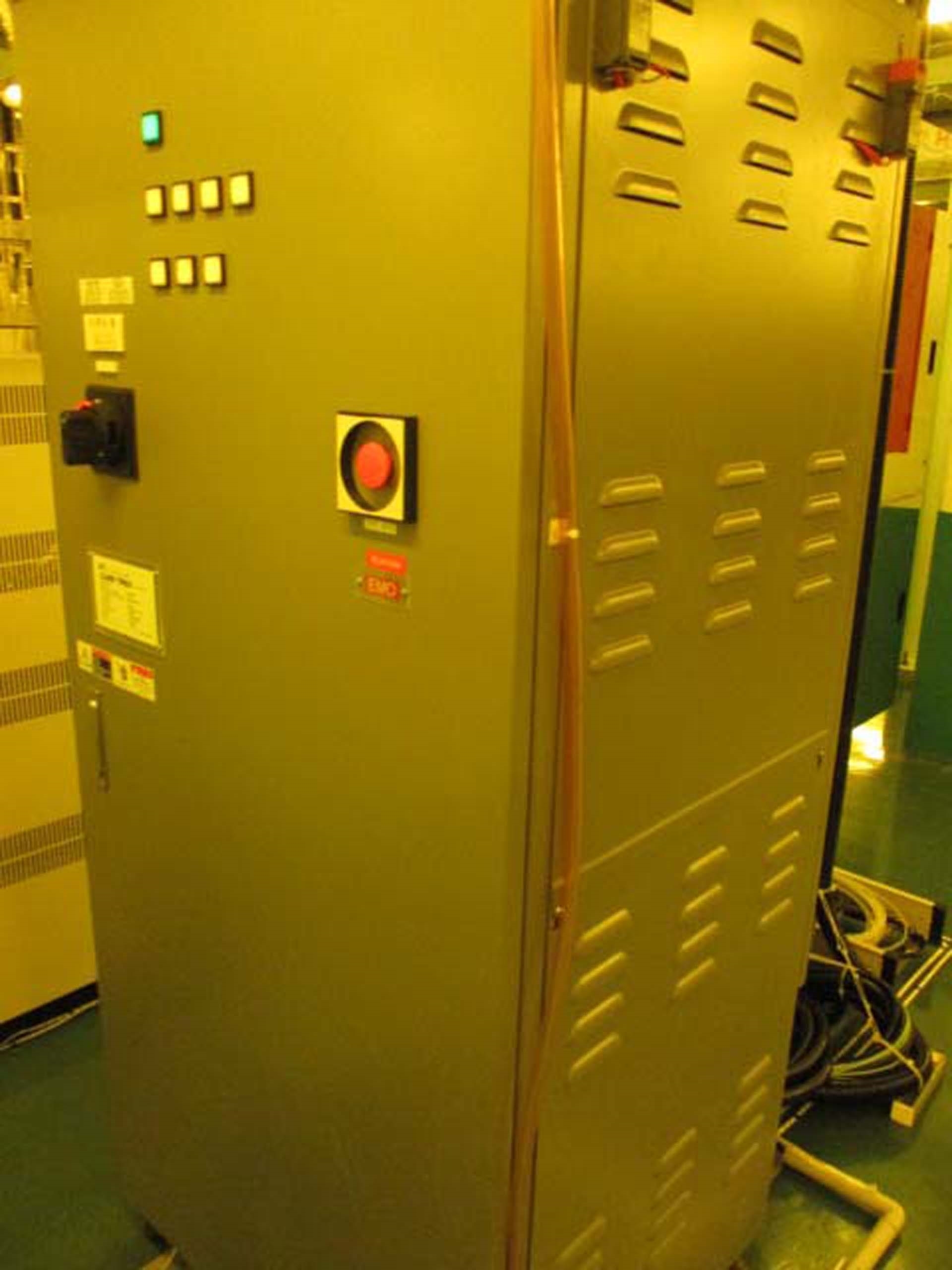

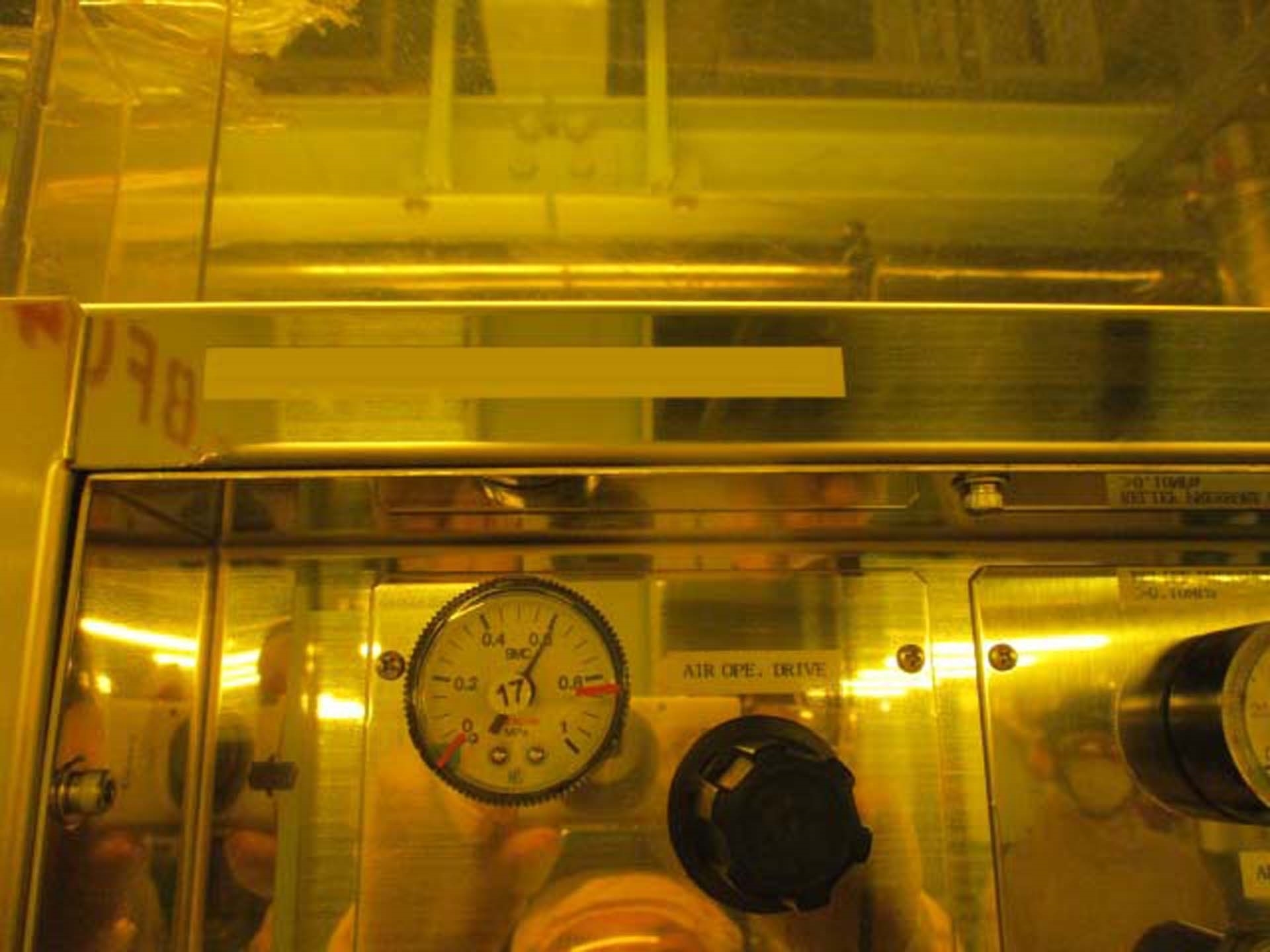


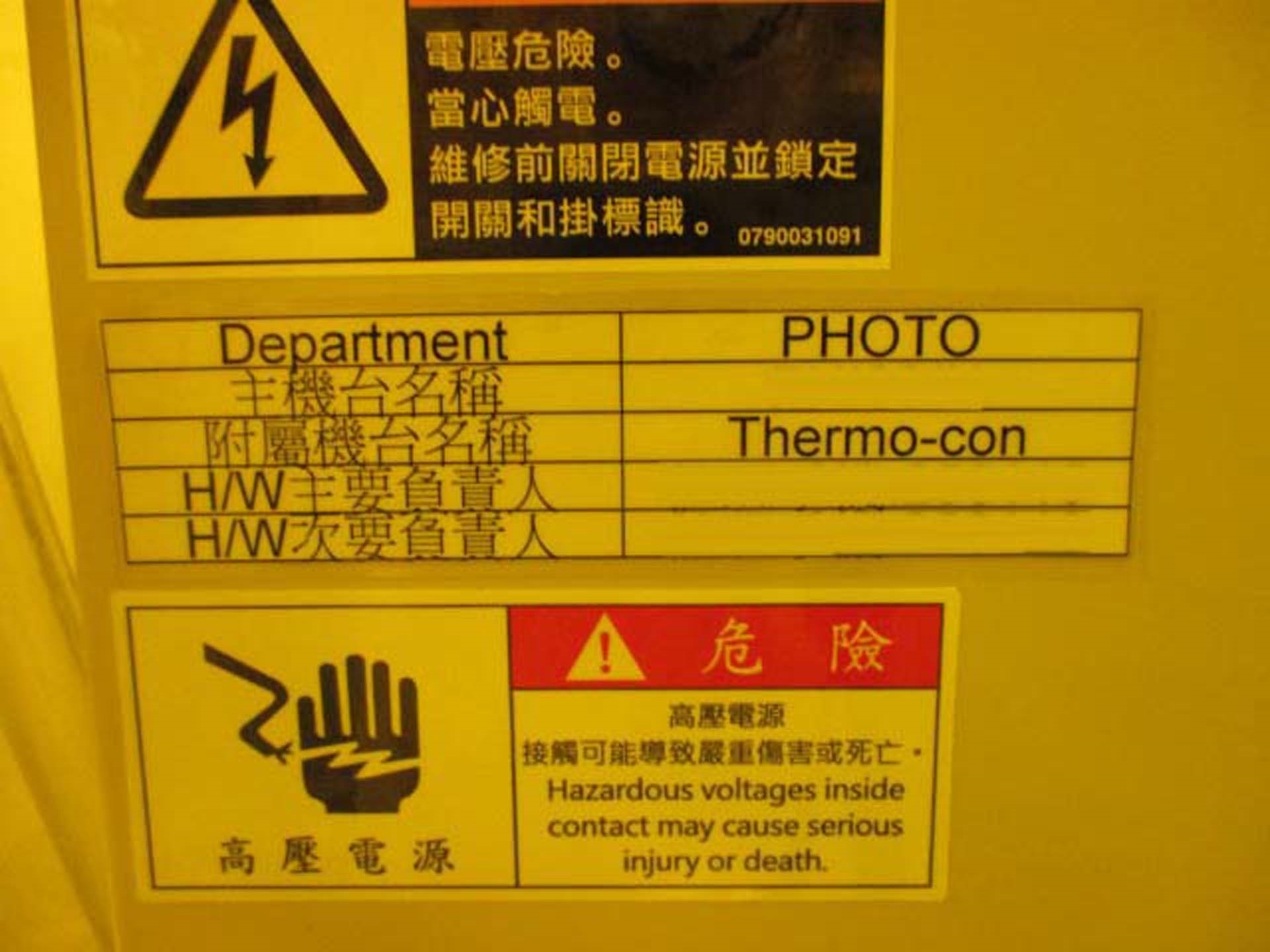

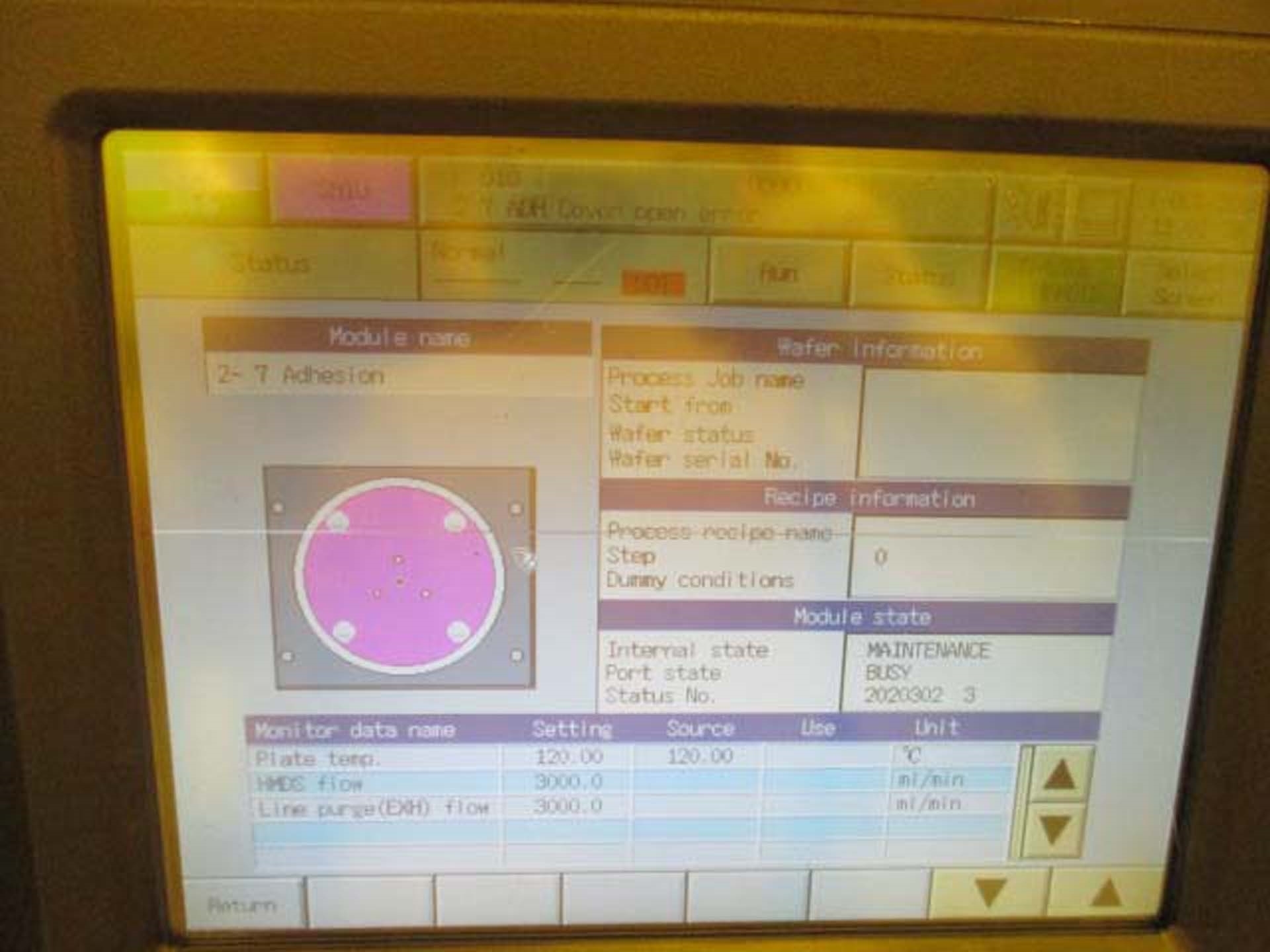








ID: 9255021
Wafer Size: 12"
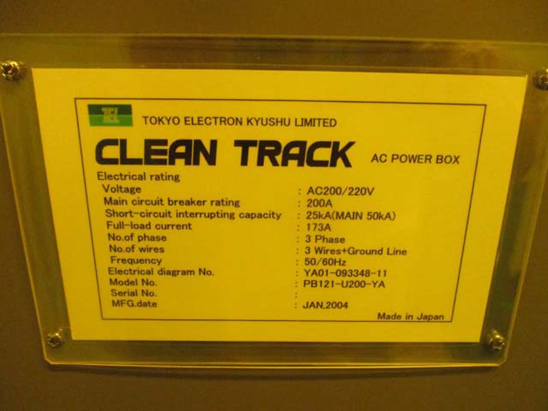
Vintage: 2004
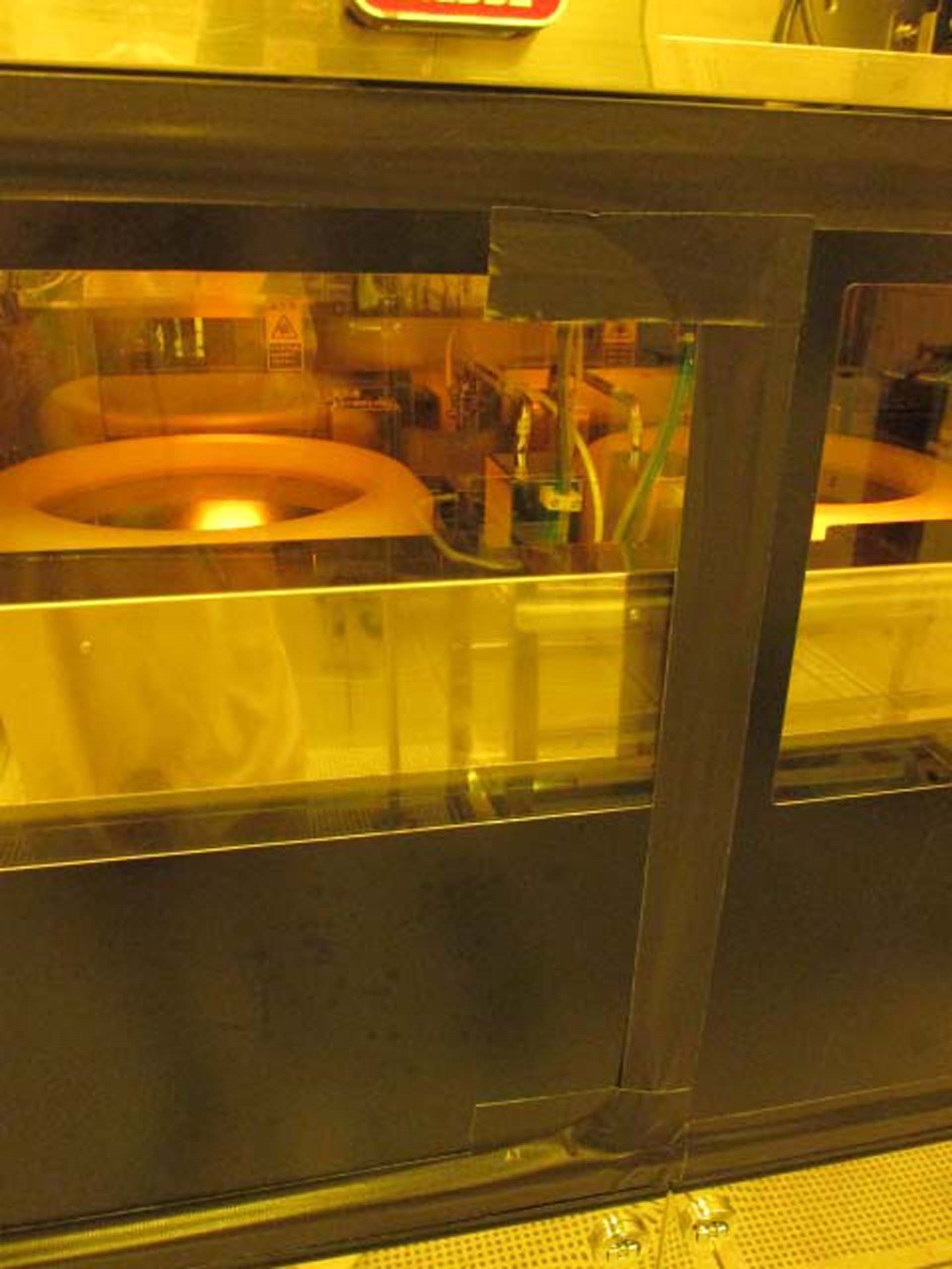
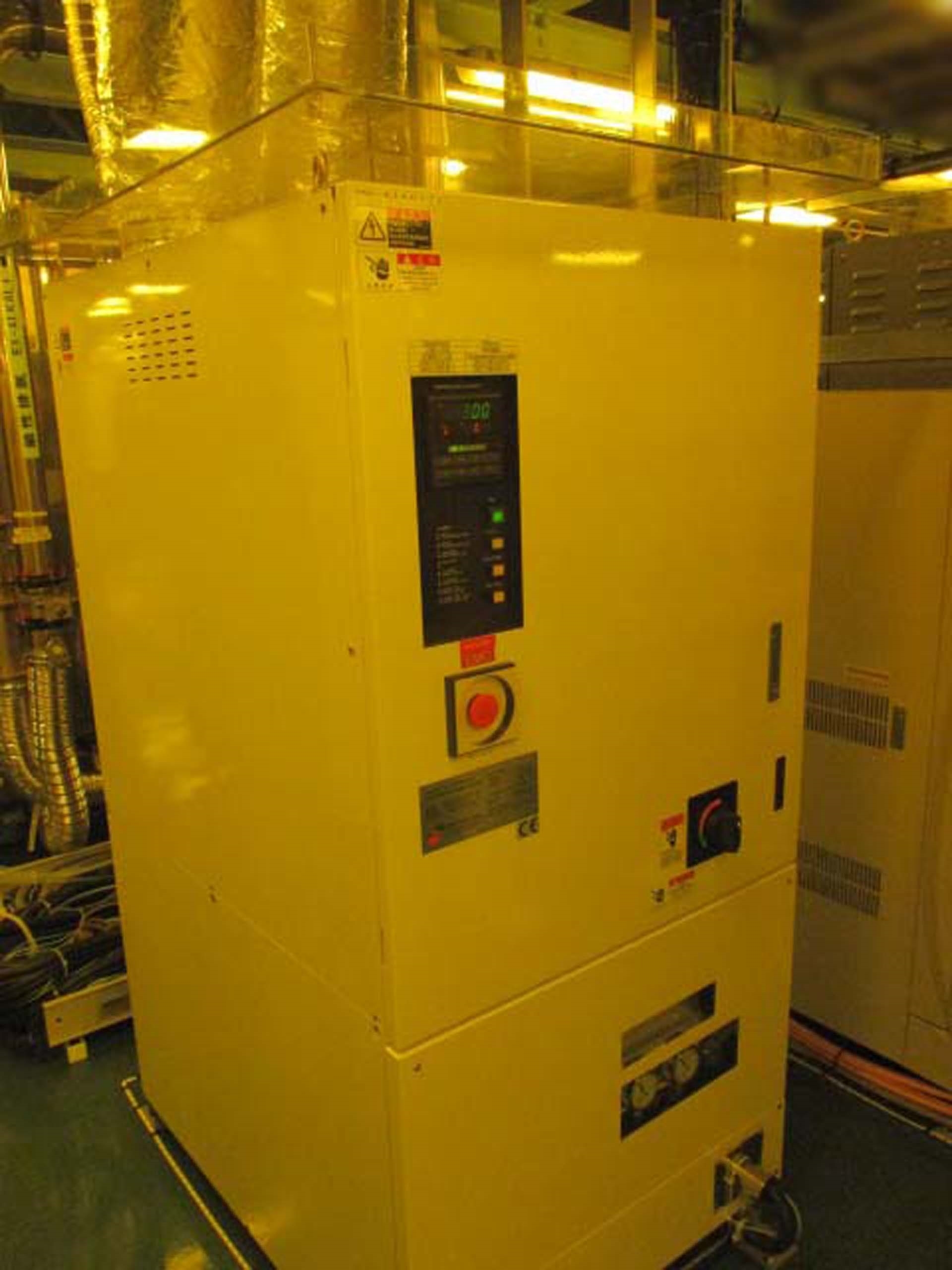
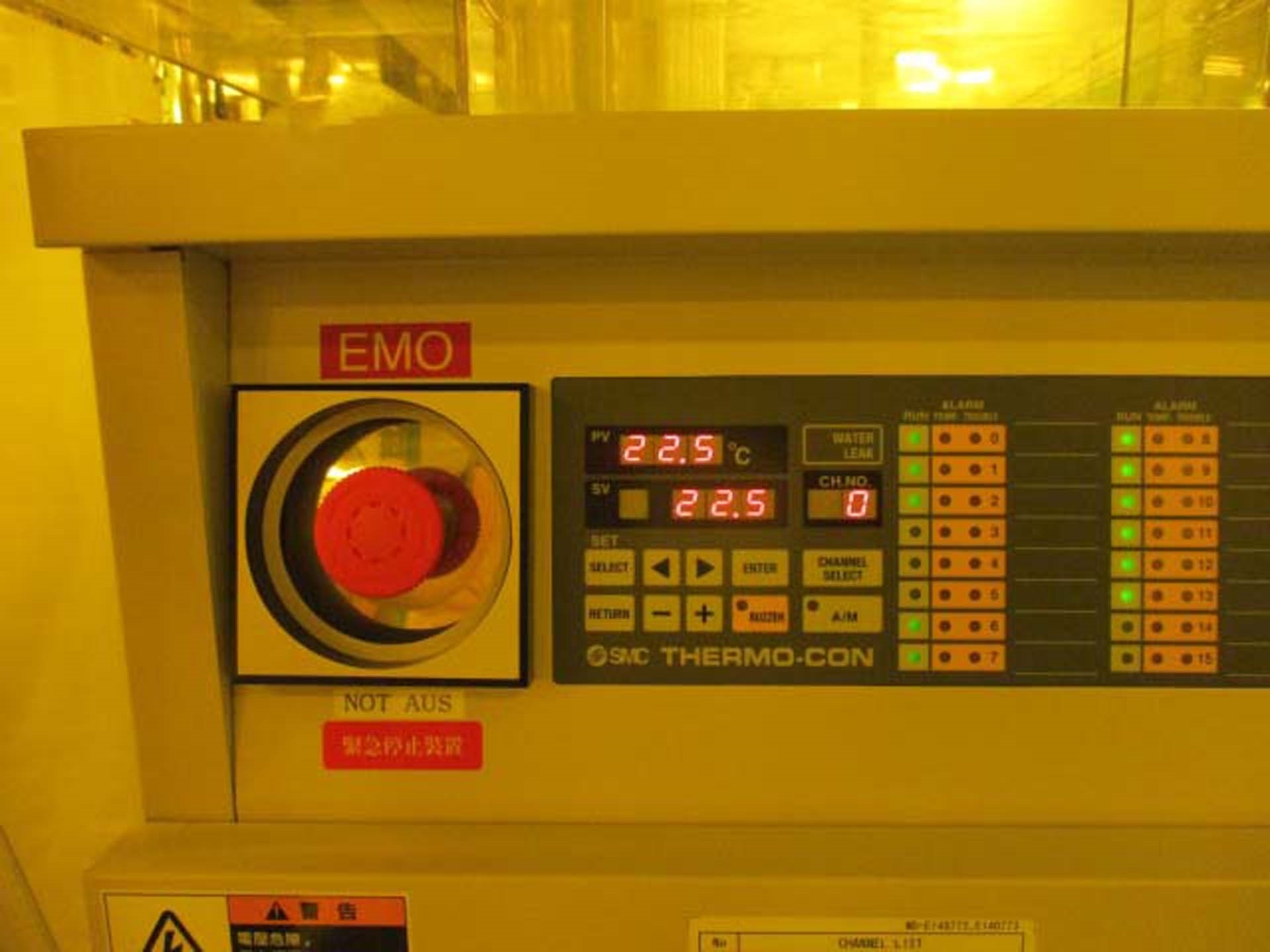
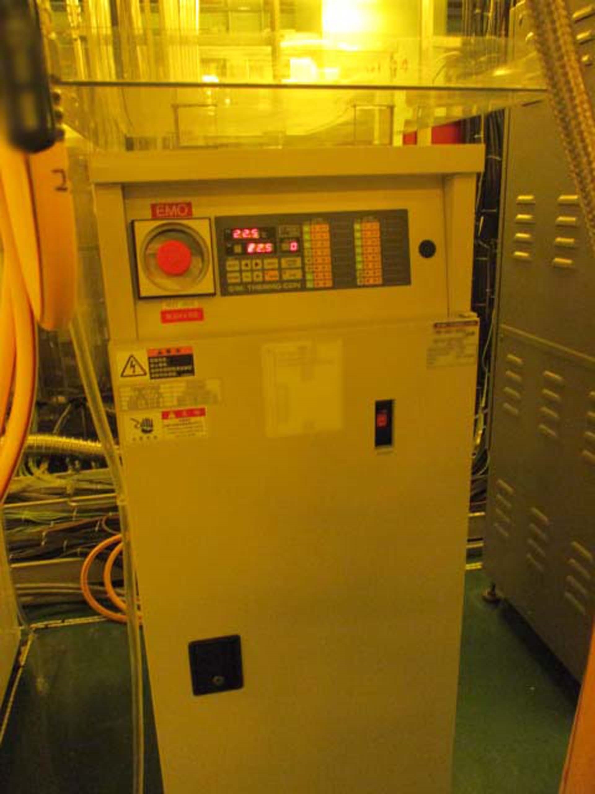
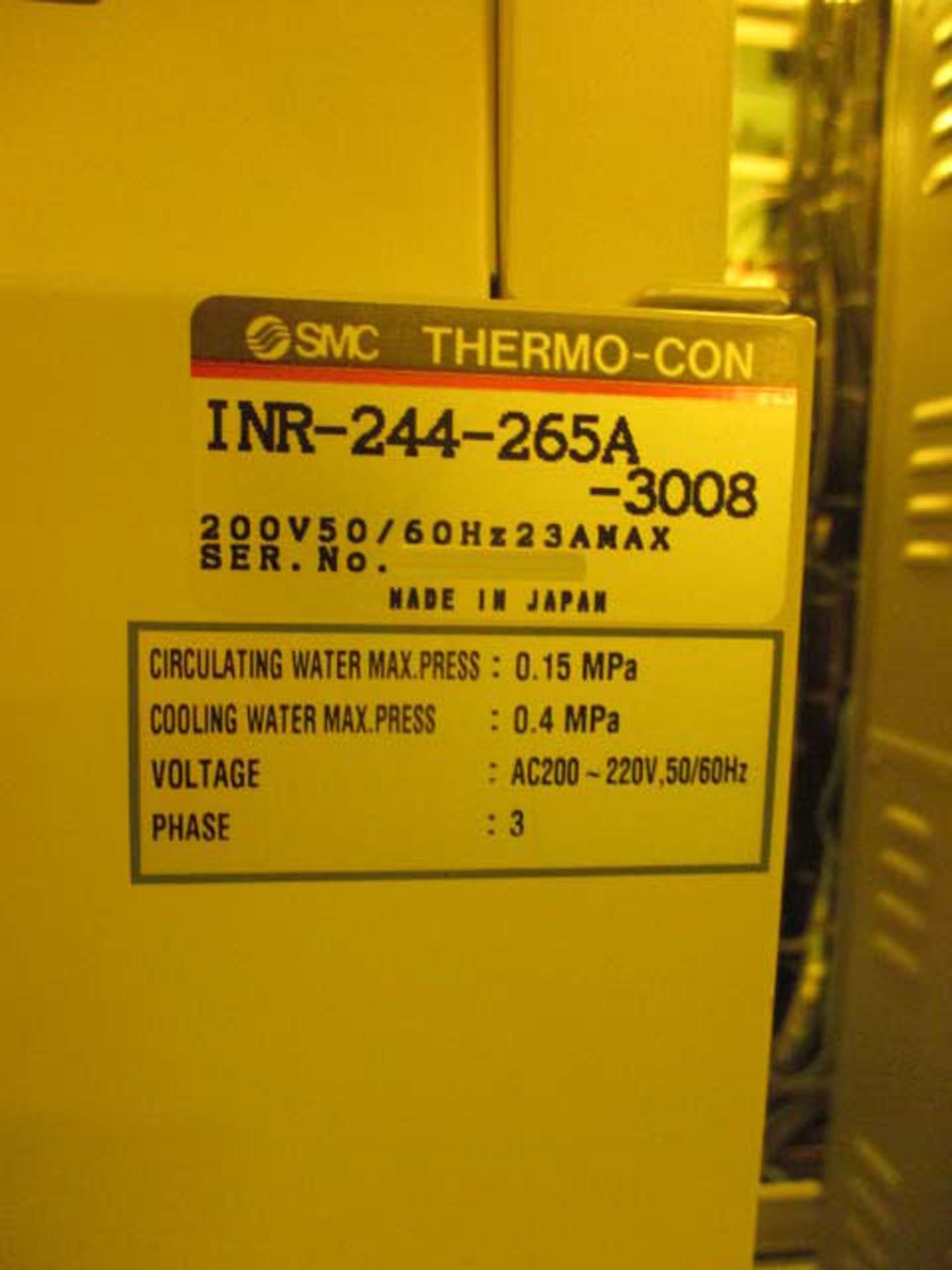
Coater / Developer system, 12"
(4) Load ports
(4) Spin modules
(22) Plates
2004 vintage.
TEL / TOKYO ELECTRON ACT 12 is a photoresist equipment used in photolithography and etching processes. This system is used primarily in producing printed circuit boards, as it allows for very precise patterning of the substrate material. The unit is composed of a photoresist layer, contact mask, exposure unit, and developer unit. The photoresist layer is the element which the light or radiation interacts with. The photoresist layer is a thin layer of material which is sensitive to radiation, so when light or radiation passes through the contact mask, it reacts with the photoresist to cause a chemical change. This transform is specific to the energy level of the radiation, so using a contact mask with various different levels of energy allows for selective removal and alteration of the photoresist layers. The contact mask itself is usually composed of a glass, quartz, or metal substrate, where irradiated images are printed on. This creates selectively exposed regions on the photoresist layer, enabling the creation of specific patterns. The contact mask is placed directly over the photoresist layer. The exposure unit is the element that the contact mask is placed upon. This unit emits the radiation required to alter the photoresist. Depending on the type of radiation used and the settings, different effects can be achieved. The radiation is varied to allow for increased accuracy of the pattern being created. Finally, the last piece of TEL ACT 12 is the developer unit. This is used after the radiation exposure is complete. The developer unit works by removing exposed portions of the photoresist layer and leaving the unexposed portions intact. This allows for very precise patterning of the substrate material. In conclusion, TOKYO ELECTRON ACT12 is a complex and highly accurate photolithography machine which can be used to create precise patterns on substrates. By using a specifically tuned radiation level and contact mask, selective removal and alteration of photoresist layers can be achieved, and this allows for highly intricate printed circuit boards to be produced.
There are no reviews yet


