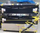
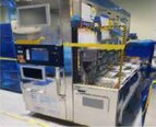
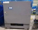
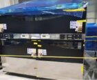
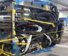
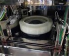
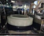
Used TEL / TOKYO ELECTRON ACT 12 #9313699 for sale
URL successfully copied!
Tap to zoom
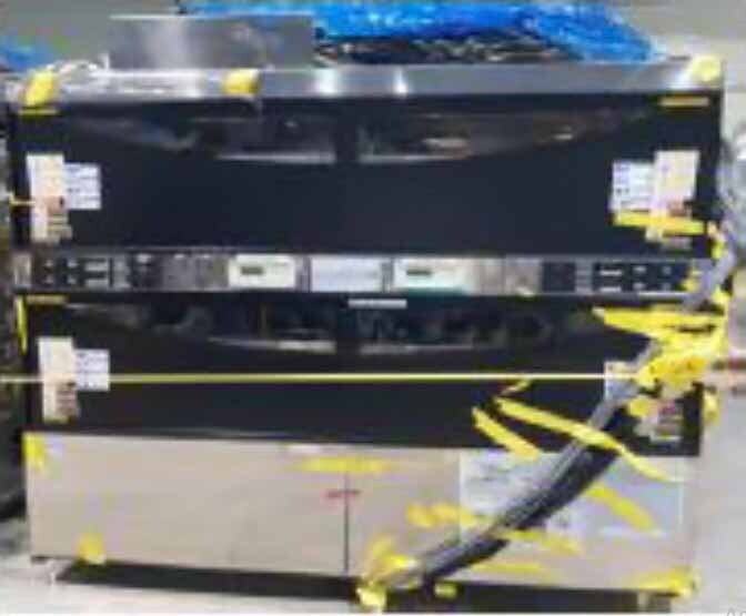

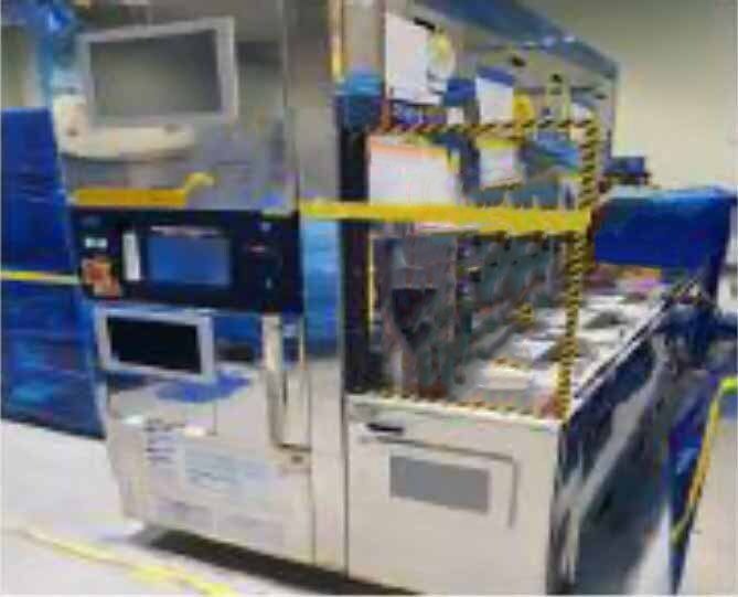

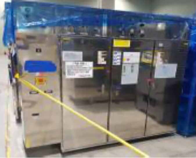

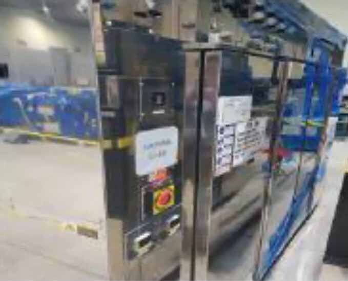


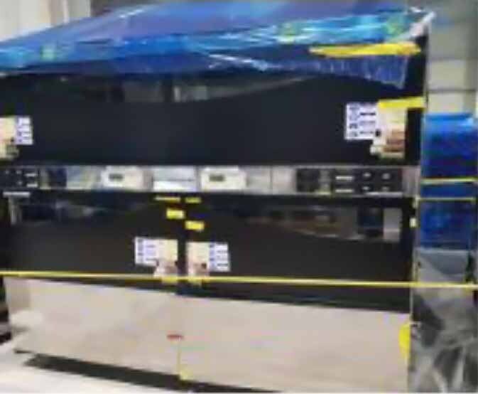

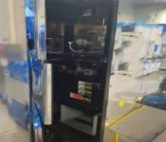










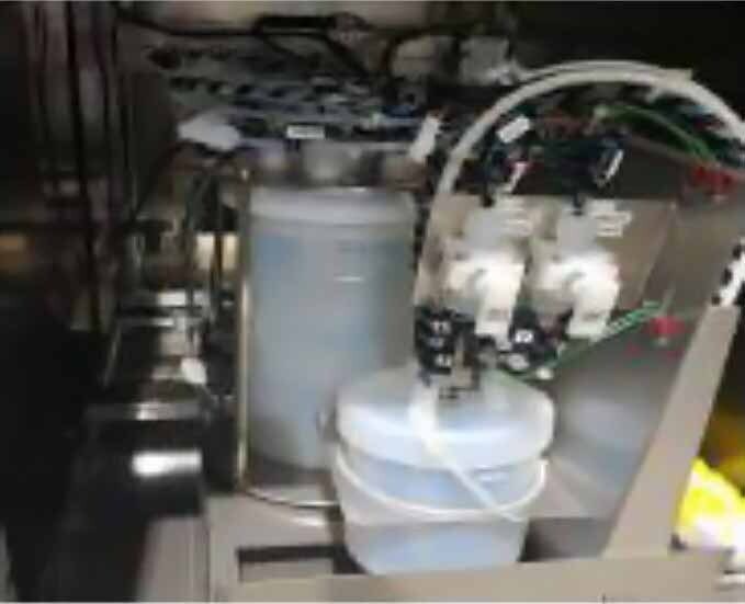


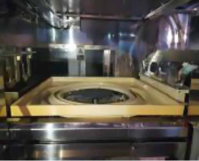

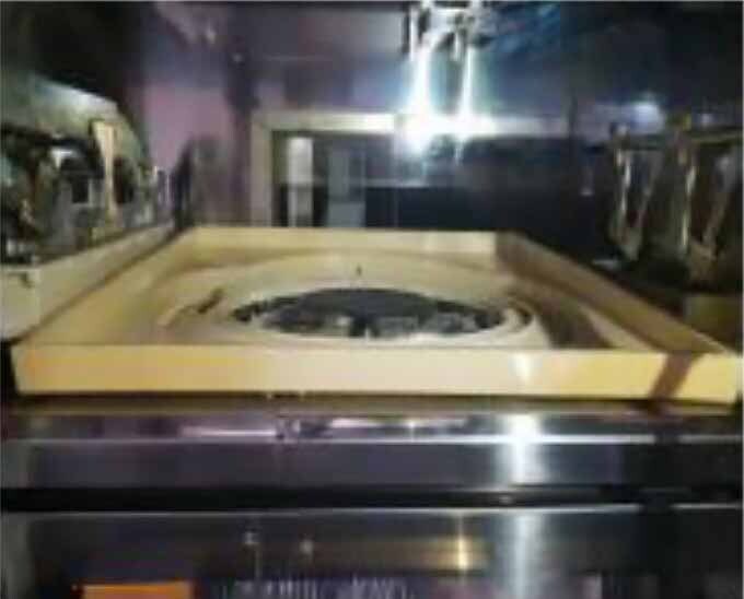














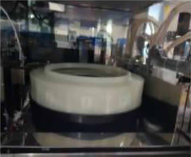



ID: 9313699
Wafer Size: 12"
Vintage: 2004
System, 12"
Wafer type: Notch
Right to left
Loading configuration: (4) Loaders
Cassette type: FOUP
Main controller missing
Main system:
Mainframe with system controller
(4) Cassettes
(25) Slots
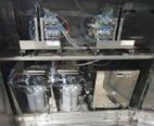
Coater unit (2-1, 2-2 Modules):
(4) Dispense nozzles with temperature controlled lines
RDS Pump
PR Suck-back valve: (8) Auto suck-back valves
Rinse nozzle: Back / EBR / Solvent bath for etch unit
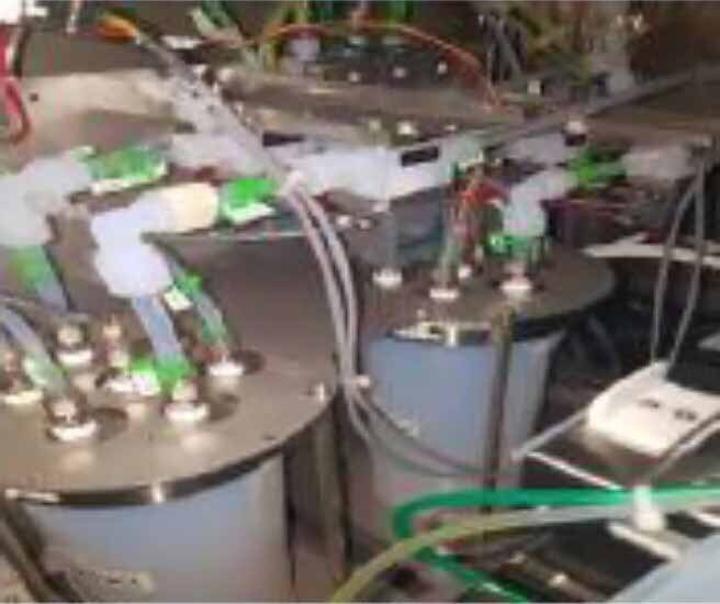
Rinse system: 3-Liters (2) buffer tank systems
Thinner supply: CCSS
Programmable side rinse:
(4) PR Nozzles
(8) Bottles: (2) Bottles / (2) Nozzles
BCT Unit (2-3,2-4 Modules):
(4) Dispense nozzles with temperature controlled line
RDS Pump
PR Suck-back valve: (8) Auto suck-back valves
Rinse nozzle: Back / EBR / Solvent bath for each unit
Rinse system: 3-Liters (2) buffer tank systems
Thinner supply: CCSS Canister tank
Developer unit (3-1, 3-2, 3-3, 3-4 Modules):
NLD Nozzle / Unit
(2) System nozzles for DI rinse
2-Points for back side rinse
Developer system: 3-Liter (2) buffer tank systems
Developer supply: CCSS
Developer temperature control system
ASML I/F Wafer stage
(2) Adhesion units (ADH):
Sealing closed chamber with Built-in hot plate
HMDS Tank with float sensor
HMDS Supply: Local bottle
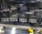
(4) Low temperature Hot Plates (LHP)
(3) High temperature Hot Plates (HHP)
(9) Chill plates (TCP)
(12) Precision Hot Plates (PHP)
(2) TRS Units
(2) Wafer Edge Exposure (WEE) Units
(2) Temperature Control Units (TCU)
OEM Type
Temperature control units (TCU) MFC controller
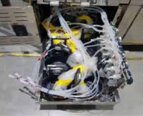
Chemical cabinets:
Cabinet 1: HNDS And solvent cabinet
Cabinet 2: DEV Solution chemical cabinet
Missing parts:
Main controller
T and H Controller
AC Power supply: 200/220 VAC, 668 A (Full-load Ampere)
2004 vintage.
TEL / TOKYO ELECTRON ACT 12 is a photoresist processing equipment designed by TEL. It is used for microfabrication and semiconductor device manufacturing processes. The system uses a photolithography process to pattern the desired features onto a wafer and etch them into a metal layer. This process involves exposing a photoresist layer, which is sensitive to UV light, to the pattern. The areas that are exposed to the light become hard, while the remaining areas remain soluble. The hard regions act as an etch mask, and the wafer is etched using the pattern formed by the photoresist layer. TEL ACT 12 provides an accurate and repeatable pattern formation process. It has a high resolution of 0.25 micron, and a field size of 5mm. The unit can also perform double-level exposure cycles in a single pass, which allows for complex patterns to be formed. The machine is designed with modularity and flexibility in mind, and offers a range of optional features that can be added to the tool to enhance its functionality. Additionally, TOKYO ELECTRON ACT12 has a fast exposure time, with an exposure time of only 2 seconds per wafer. This allows for a high throughput of wafers to be processed in a short amount of time. TOKYO ELECTRON ACT 12 also uses linear scan technology to ensure an even dose of UV light across the substrate. This allows for smoother and more accurately defined features to be formed. Furthermore, the asset has an onboard computer that contains all the relevant exposure parameters and can be customized to fit the needs of the user. Overall ACT 12 is a reliable and efficient tool for microfabrication and semiconductor device manufacturing processes. Its high resolution, fast exposure time, high throughput, flexible model design, and UV linear scanning make it an ideal choice for professionals in the industry.
There are no reviews yet
