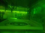
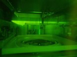
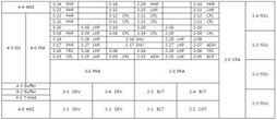
Used TEL / TOKYO ELECTRON ACT 12 #9364744 for sale
URL successfully copied!
Tap to zoom
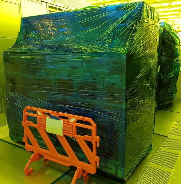

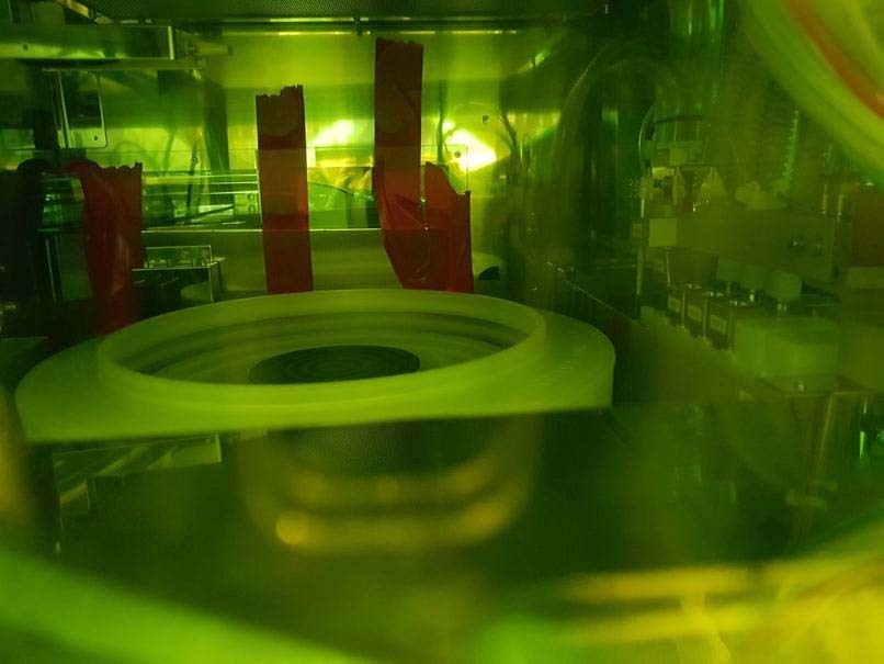


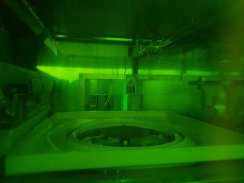

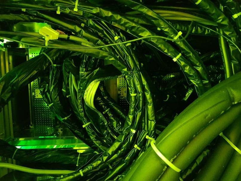


ID: 9364744
Wafer Size: 12"
Vintage: 2004
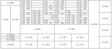
(4) Coater / (4) Developer system, 12"
Wafer type: Notch
Right to left
Loading configuration: (3) Uni cassettes
Cassette type: FOUP
Inline
CSB
PRB1
PRB2
IFB
AC Power box
(2) Chemical boxes
Main controller
25-Slots
Coater unit (2-1, 2-2 Modules):
(4) Dispense nozzles with temperature controller lines
RDS Pump
PR Suck-back valve: (8) Auto suck-back valves
Manual drain
Programmable side rinse: CCSS Thinner supply
BCT Unit (2-3,2-4 Modules):
(2) Dispense nozzles with temperature controller line
RDS Pump
PR Suck-back valve: (4) Auto suck-back valves
Rinse system: 3-Liters (2) buffer tank systems
Manual drain
Programmable side rinse:
Thinner supply: CCSS
Developer unit (3-1, 3-2, 3-3, 3-4 Modules):
NLD Nozzle / Unit
(2) Stream nozzles for DI rinse
2-Points for back side rinse
Developer system: 3-Liter (2) buffer tank systems
Developer supply: CCSS
Developer temperature controller
Direct drain
ASML I/F Wafer stage
Temperature Control Unit (TCU)
(2) Chemical cabinets
T and H Controller missing
Power supply: AC 208 V, 3 Phase
2004 vintage.
TEL / TOKYO ELECTRON ACT 12 photoresist equipment is one of the leading systems for semiconductor device fabrication. This system is designed for the development and production of thin films used in the manufacturing of semiconductor devices such as CPUs, GPUs, memories, and other components. It provides precise thin film processing required for advanced device integration and features high-performance capabilities for fine-tuning thin film formation. TEL ACT 12 unit is equipped with a powerful electron beam for photoresist patterning and a high-precision exposure stage for precise positioning and patterning of the thin film. With the use of the unique Dual Beam Mapping Machine (DBMS) the tool is able to deliver high levels of uniformity and accuracy in thin film formation. The DBMS enables simultaneous detection and analysis of the electron beam dose distribution across the entire area of the sample, providing a high-resolution view of the thin film pattern. TOKYO ELECTRON ACT12 also features a high-precision stage and multiple patterning algorithms for optimising pattern generation, as well as powerful software for monitoring and diagnosing exposure conditions. The asset supports a wide variety of photoresist materials and enables the processing of different patterns of complex structures. The model also supports a range of other options, including thermal control, multi-axis alignment and component protection. With its combination of precision, performance and advanced features, ACT12 photoresist equipment is the perfect solution for high-end semiconductor device fabrication. The system provides the highest levels of performance and accuracy, enabling device makers to produce the finest and most advanced semiconductor devices on the market. It also offers an extremely low cost of ownership, making it an ideal choice for any production environment.
There are no reviews yet

