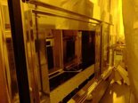
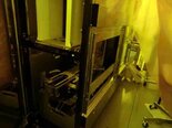
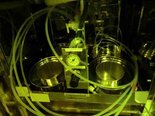
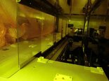
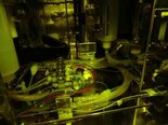
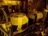
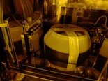
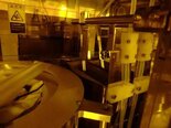
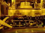
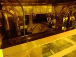
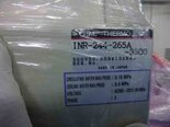
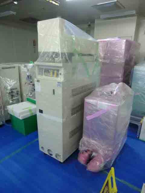
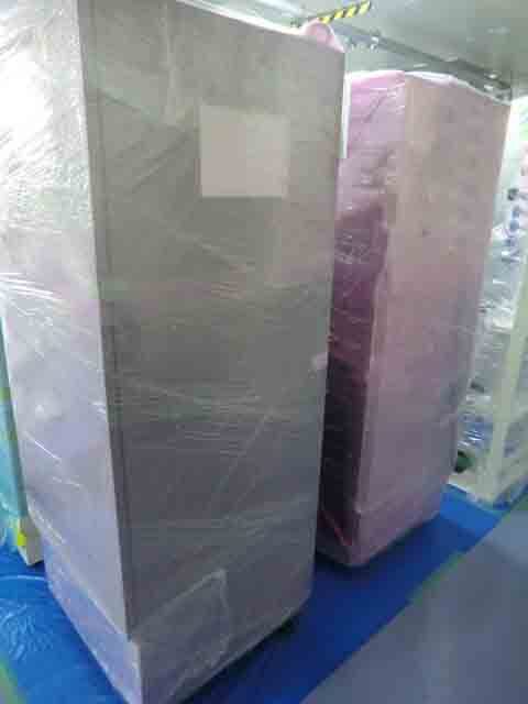
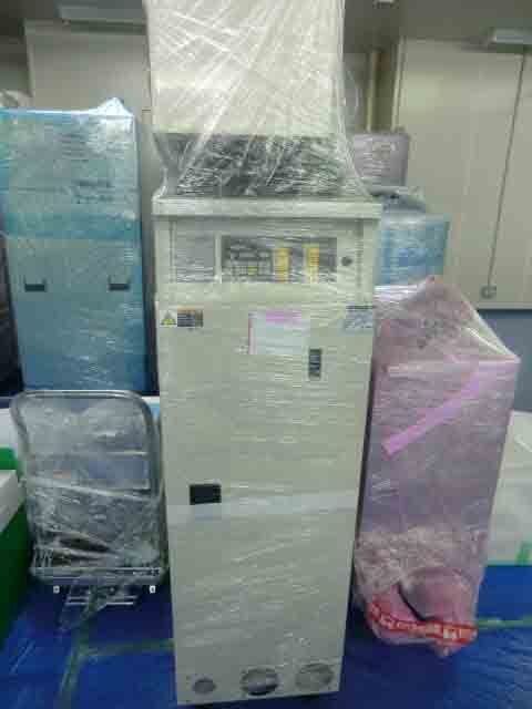
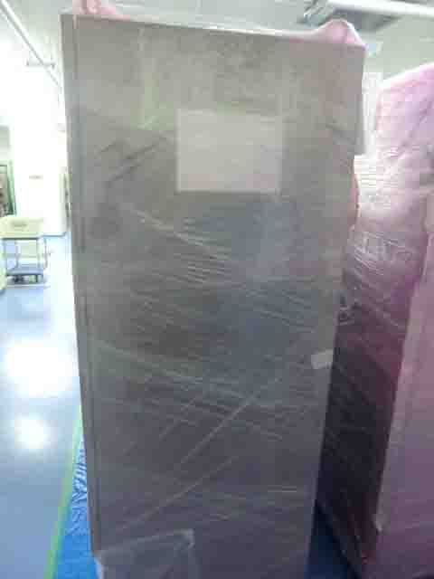
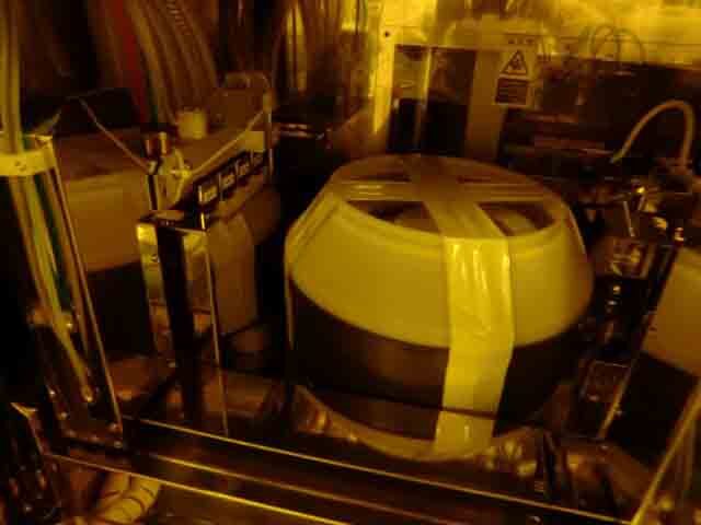
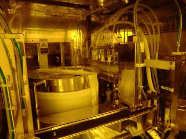
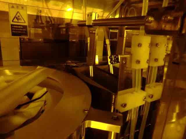
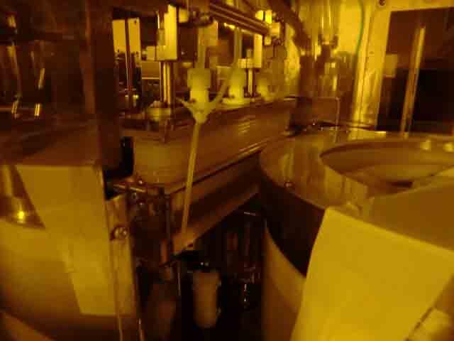
Used TEL / TOKYO ELECTRON ACT 8 #293610442 for sale
URL successfully copied!
Tap to zoom
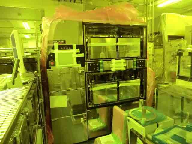






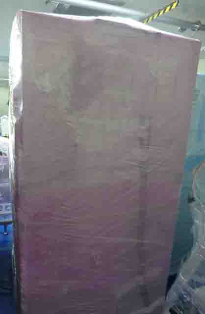


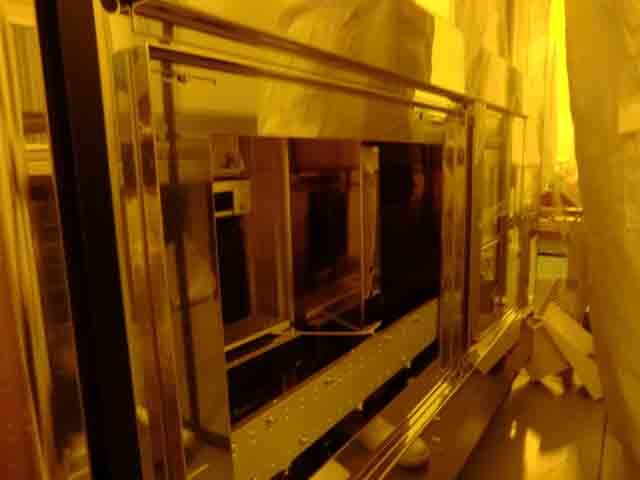


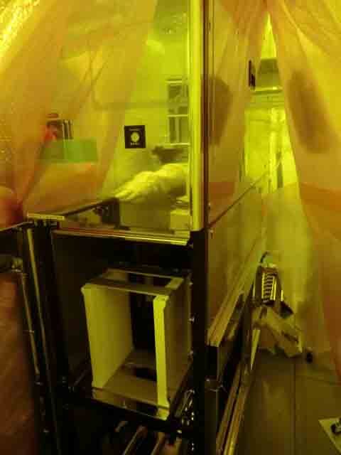

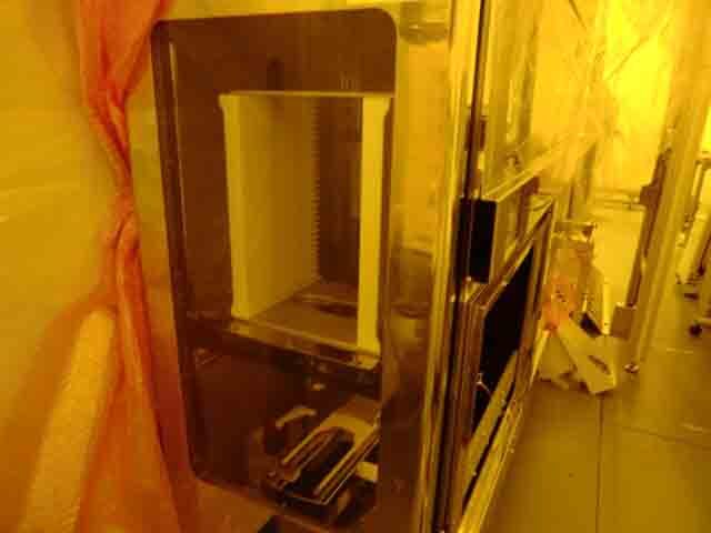






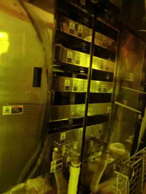


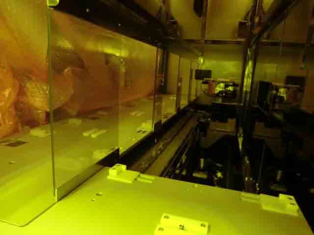

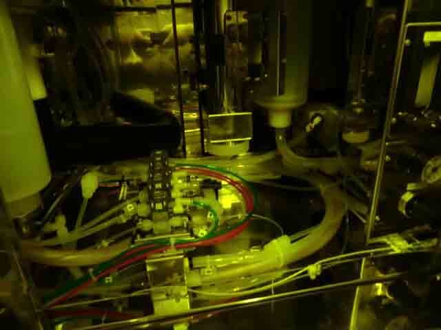

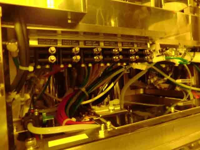











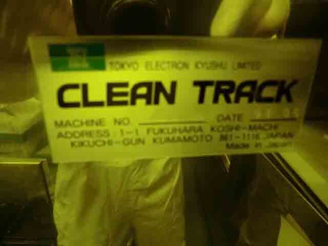

ID: 293610442
Wafer Size: 8"
Vintage: 2004
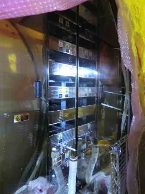
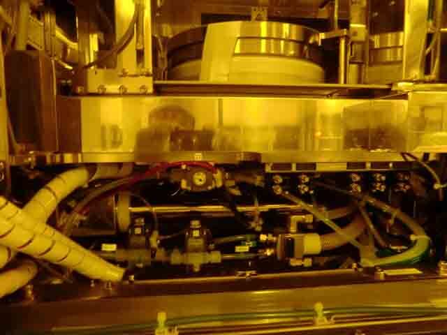
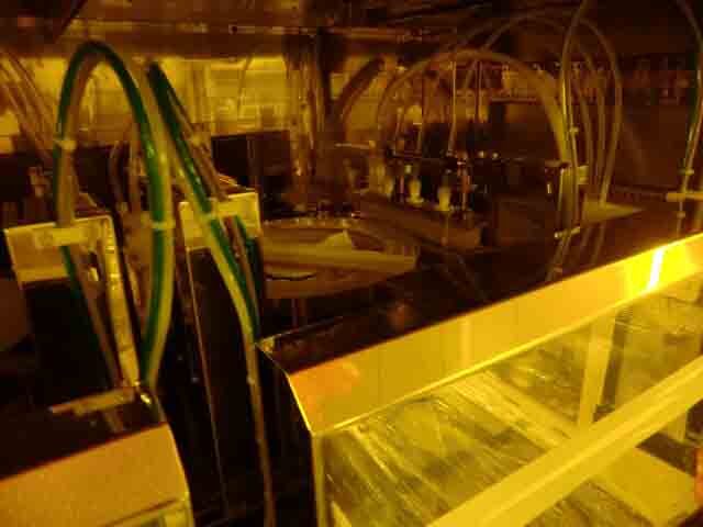
(2) Coater / (2) Developer system, 8"
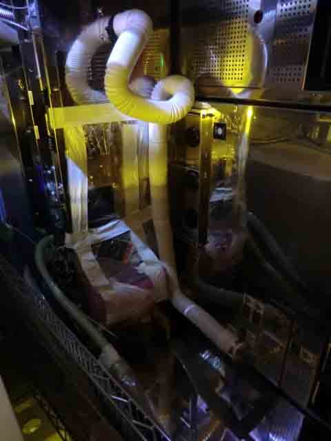
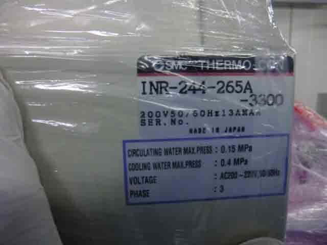
Chiller
Chemical box
Power box
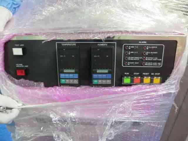
Temperature and humidity controller
Signal tower: (3) Lights
Open cassette carrier
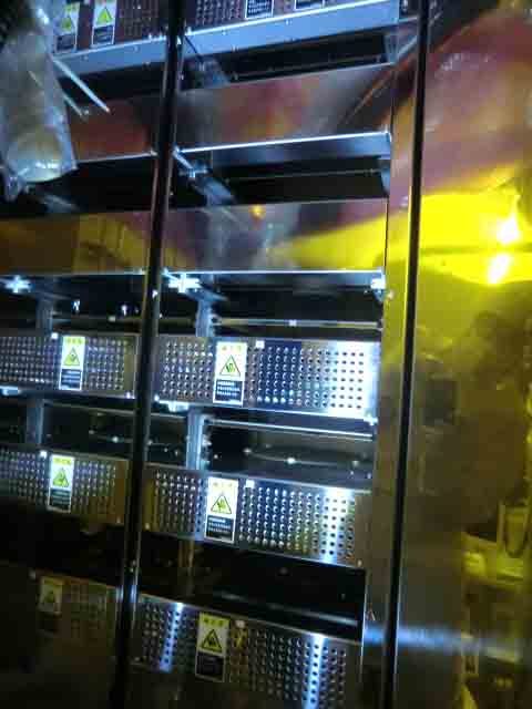
Bake board type / Cooling board type: Proximity, Spacer
Solvent supply method: Canister automatic switching, 10 L
DEV Cup: PP+POM
Modules:
I/F
ADH
(3) TRS
(3) CPL
(6) LHP
CWH
WEE
(4) STG
DEV Nozzle:
E2 Nozzle
Rinse
Back rinse
2004 vintage.
TEL / TOKYO ELECTRON ACT 8 is a photoresist equipment developed by TEL, one of the leading manufacturers of semiconductor fabrication equipment in the world. The system is capable of creating circuits and other patterns on wafers with a resolution of 5µm. It is a multi-patterning photoresist unit that can pattern multiple layers in a single exposure. TEL ACT 8 has a large wafer capacity, from 12" to 24", and is capable of processing large volumes of substrates simultaneously. Its advanced optics machine allows for precise and uniform patterning. Its high speed scanner can move substrates faster and with higher accuracy than previous models. It features precise plasma dosing technology for better edge placement accuracy and can accommodate high-speed arc programming for precise patterning. TOKYO ELECTRON ACT 8 tool also has excellent wafer alignment capabilities, thanks to its advanced numerical aperture asset. Furthermore, wafers can be inspected more closely via its built-in optical microscopy, which can be used to find defects or observe the surface of the substrate. The model also offers low particle contamination and tight particle control. It is equipped with an auto-scanning particle detector to ensure a cleaner environment and to monitor the size and amount of particles present in the equipment. Along with the particle detector, the system can also reduce the amount of contamination caused by moisture and clean room air. Furthermore, the unit is fitted with a temperature control machine that can ensure a stable environment for product processing and reduce thermal drift during product exposure. This feature also minimizes film shrinkage and increases production yields. TOKYO ELECTRON ACT 8 tool is an ideal solution for some of the most advanced photoresist processes in the semiconductor industry. Its superior resolution capabilities and tight control over film thickness have made it one of the most reliable and consistent photoresist systems available. With its advanced features and capabilities, ACT 8 asset is an excellent choice for all photoresist needs in the production of integrated chips.
There are no reviews yet


