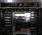
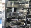
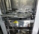
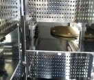
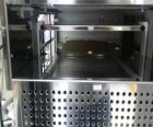
Used TEL / TOKYO ELECTRON ACT 8 #9151698 for sale
URL successfully copied!
Tap to zoom
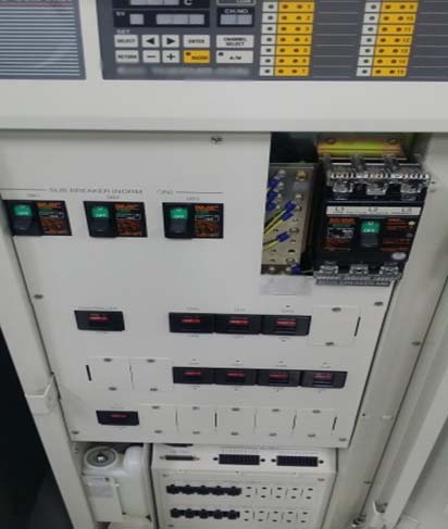

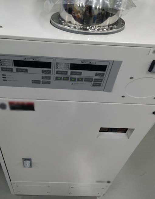

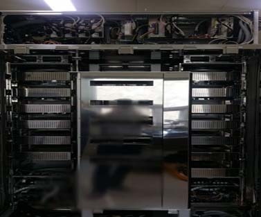

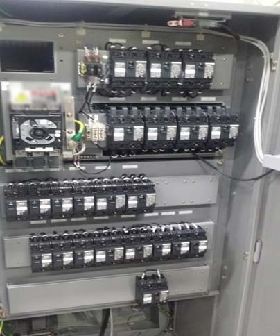

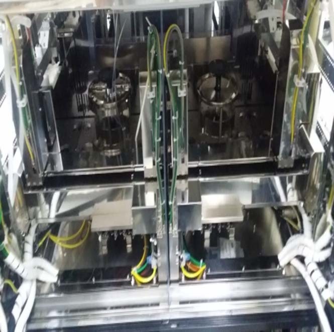

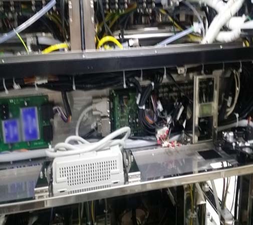

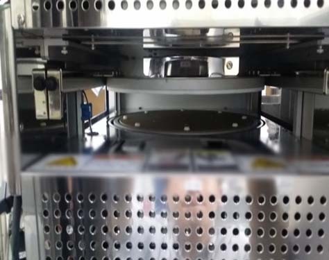

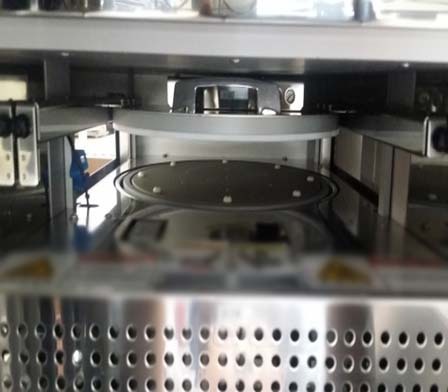

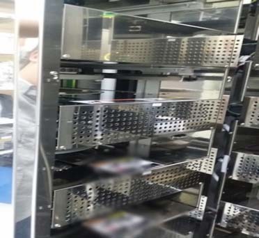

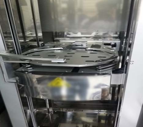


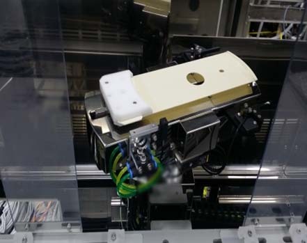

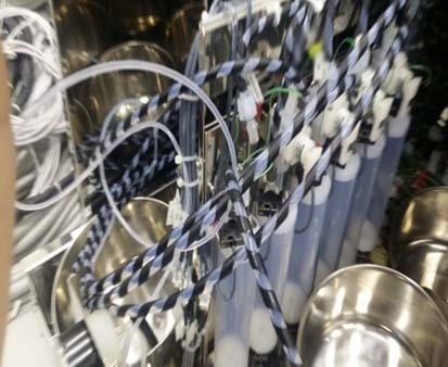






ID: 9151698
Wafer Size: 8"
Coater / developer system, 8"
Carrier station type: Open cassette
Wafer loading type: Left to right
Coater unit:
2-1 Unit:
Coater type: Coater
Pump model: RRC
(3) Nozzle count
Suck back valve
Spin motor: Yasgawa
2-2 Unit:
Coater type: Coater
Pump model: RRC
(3) Nozzle count
Suck back valve
Spin motor: Yasgawa
Develop unit:
2-3 Unit:
(2) Dev nozzle count
Up/Down move: Cylinder
Spin motor: Parasonic
2-4 Unit:
(2) Dev nozzle count
Up/Down move: Cylinder
Spin motor: Parasonic
(10) Low temp hot plates (LHP)
(5) Chill plate (CPL)
Chilling hot plate (CHP)
Cup wash holder (CWH)
(1) Transition (TRS)
(1) Transition chill plate (TCP)
Sub module:
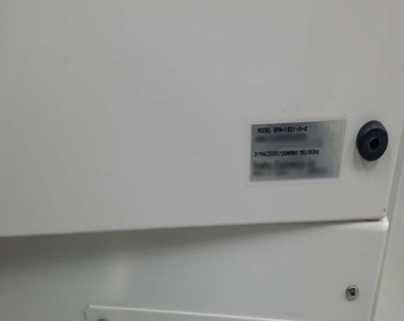
THC Maker & model: KOMATS SPA-1821
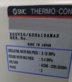
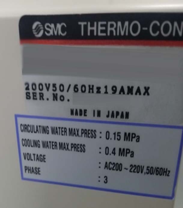
TCU Maker & model: SMC TEL Standard
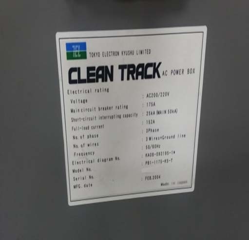
AC Power box capacity: AC 208 3θ 125A
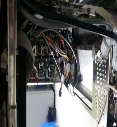
Missing parts:
Main controller
2-3,2-4 Dev solution nozzle assy
2-3,2-4 Dev drain pipe assy
2-1,2-2 Resist suck back valve
2-3 Dev spin driver
Dev & cot cup assy
Chemical cabinet parts
IFB Block
2-15 CPL
2-16 TRS.
TEL / TOKYO ELECTRON ACT 8 is a photoresist equipment designed specifically for the production of lightweight integrated circuit (IC) substrates. This system makes use of a photoresist layer in order to create the masks necessary for subsequent lithography step. This layer allows light sensitivity to be tailored to specific wavelengths, meaning that the ICs can be produced with greater precision. The main components of TEL ACT 8 are the exposure module, which contains the photomask, a spinning chuck and stage, and a UV laser. The UV laser is used to generate a pattern of varying intensity onto the photoresist layer. This pattern is created by the spinning chuck and stage, which is used to move the photomask under the UV laser. The pattern is then exposed onto the integrated circuit substrate, which is then processed further by the other components of the machine. In order to ensure precision and accuracy in the production of the ICs, TOKYO ELECTRON ACT 8 also has a highly sensitive Imaging unit. This machine takes a detailed scan of the photoresist layer after it has been exposed, to ensure that any changes in the pattern are detected and can be attended to. Additionally, the tool contains an advanced metrology control unit, which has the capability to measure up to 0.1 microns in order to ensure accuracy. The asset is also capable of contact exposure, where the photoresist layer acts as a negative mask in order to transfer images directly onto the integrated circuit substrate. This method is used when highly precise masks are needed or when small features need to be generated at a high yield. TOKYO ELECTRON ACT 8 is a highly advanced photoresist model designed to create the masks necessary for subsequent lithography step. This equipment contains an exposure module, Imaging system and metrology control unit, all of which work together to ensure the precision and accuracy necessary for the production of lightweight ICs. This unit is able to contact exposure and is capable of generating images up to 0.1 microns in size.
There are no reviews yet


