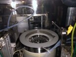
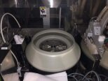
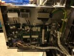
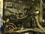
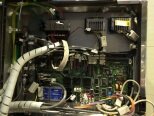
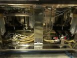
Used TEL / TOKYO ELECTRON ACT 8 #9241944 for sale
URL successfully copied!
Tap to zoom


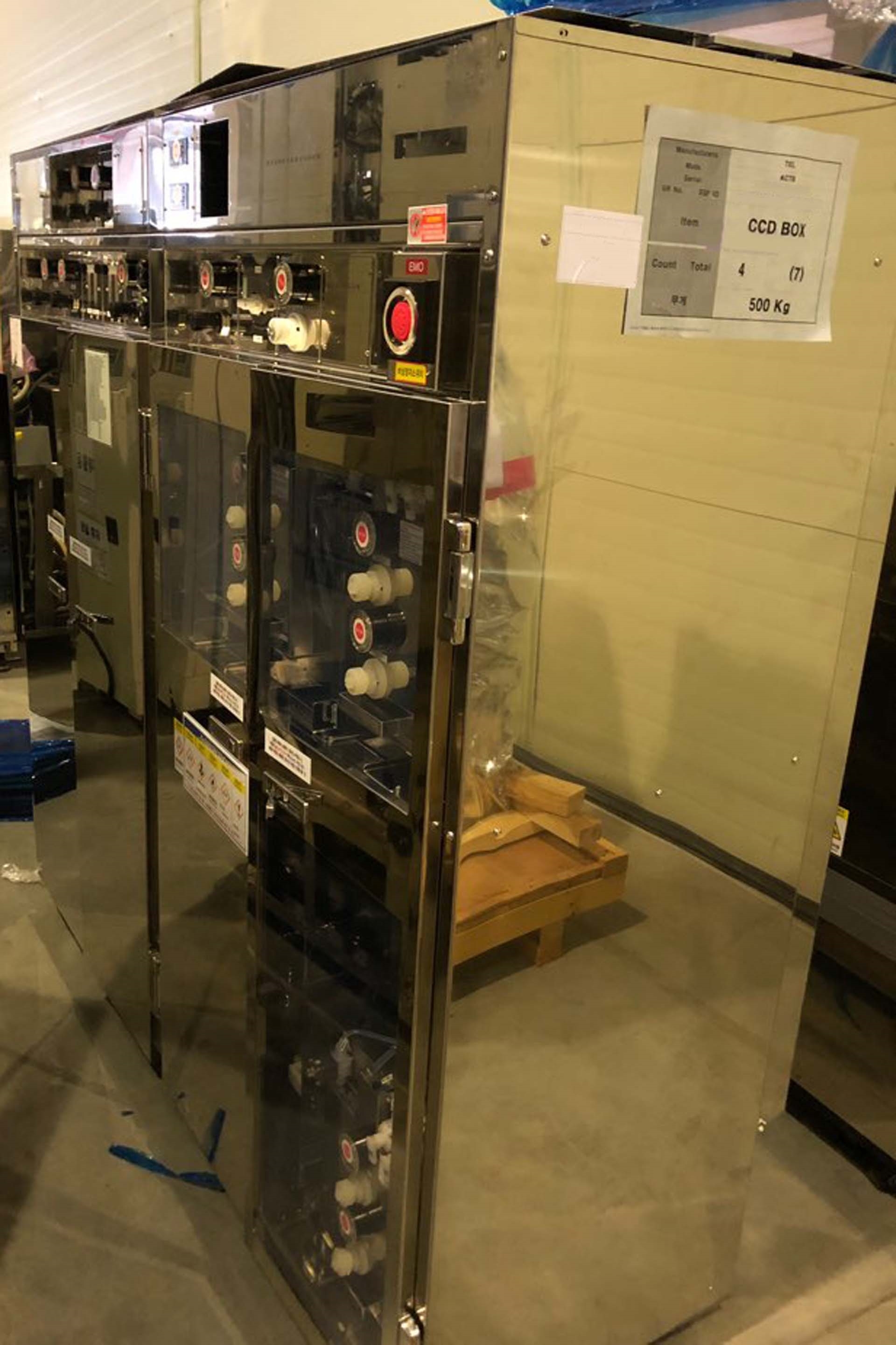


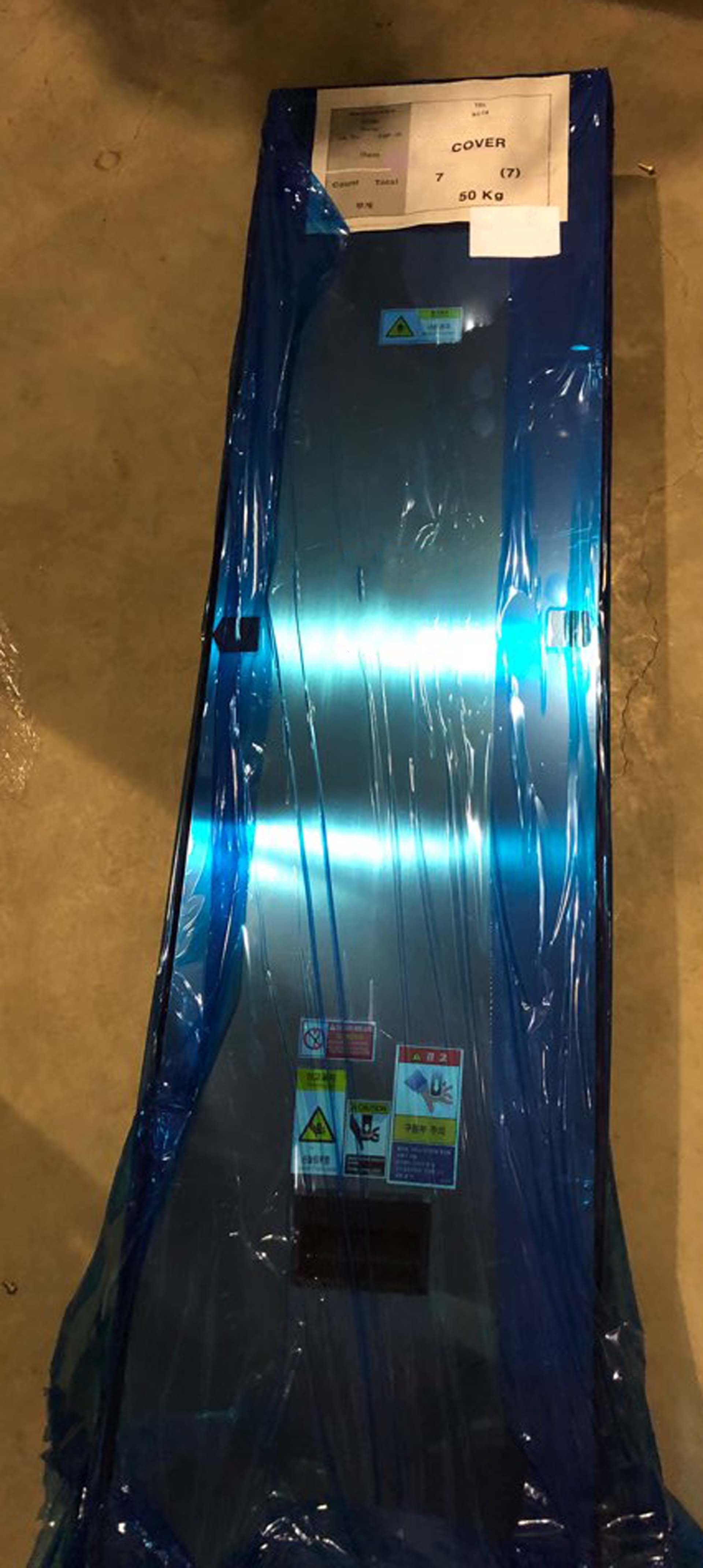

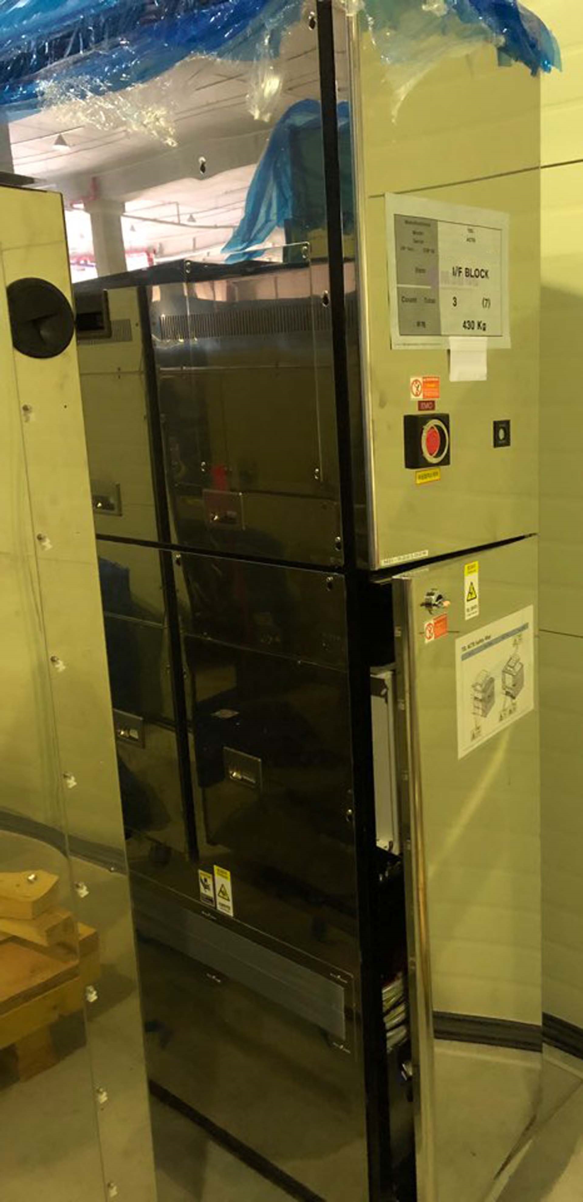

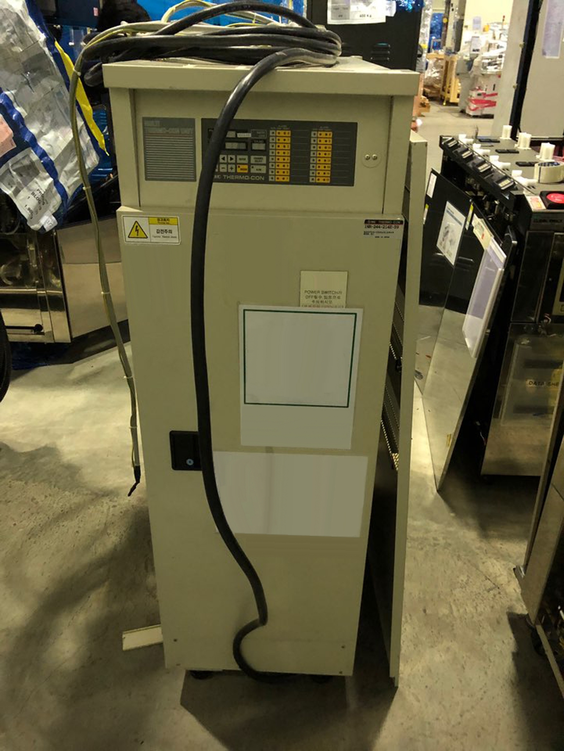

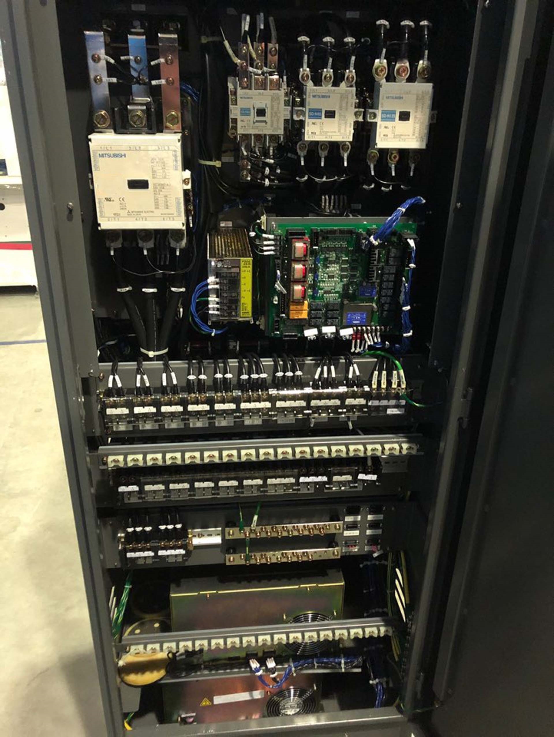

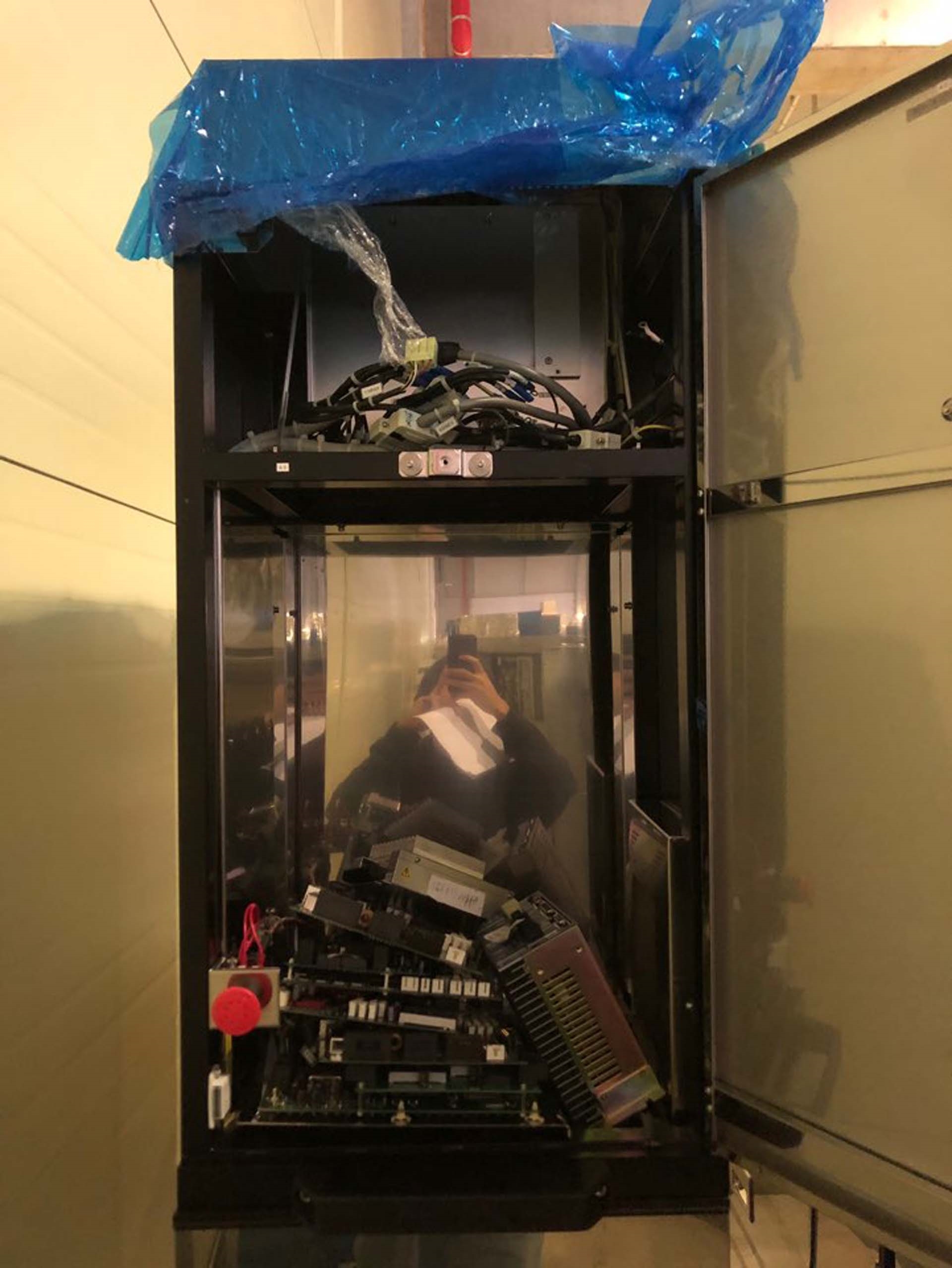

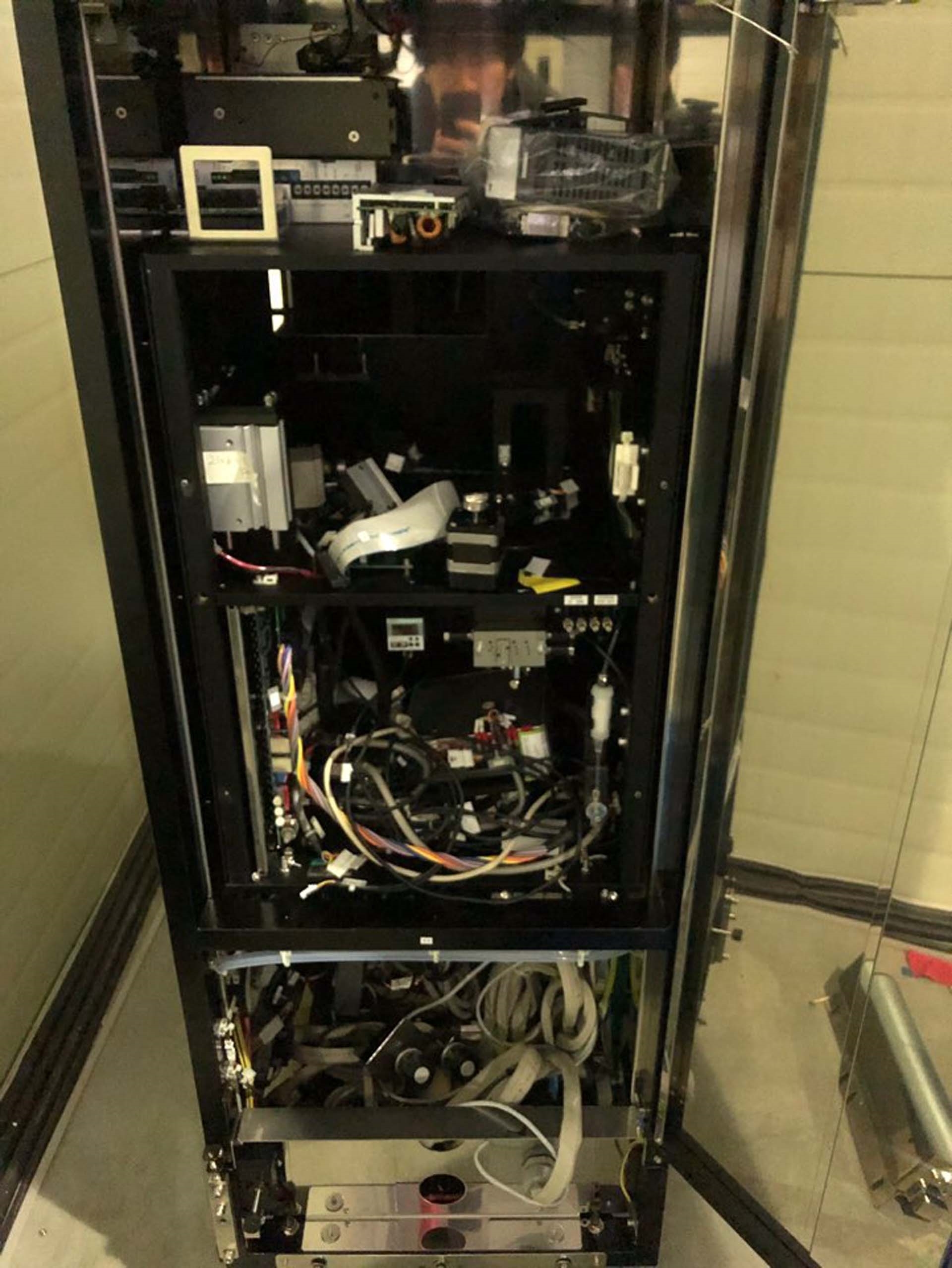


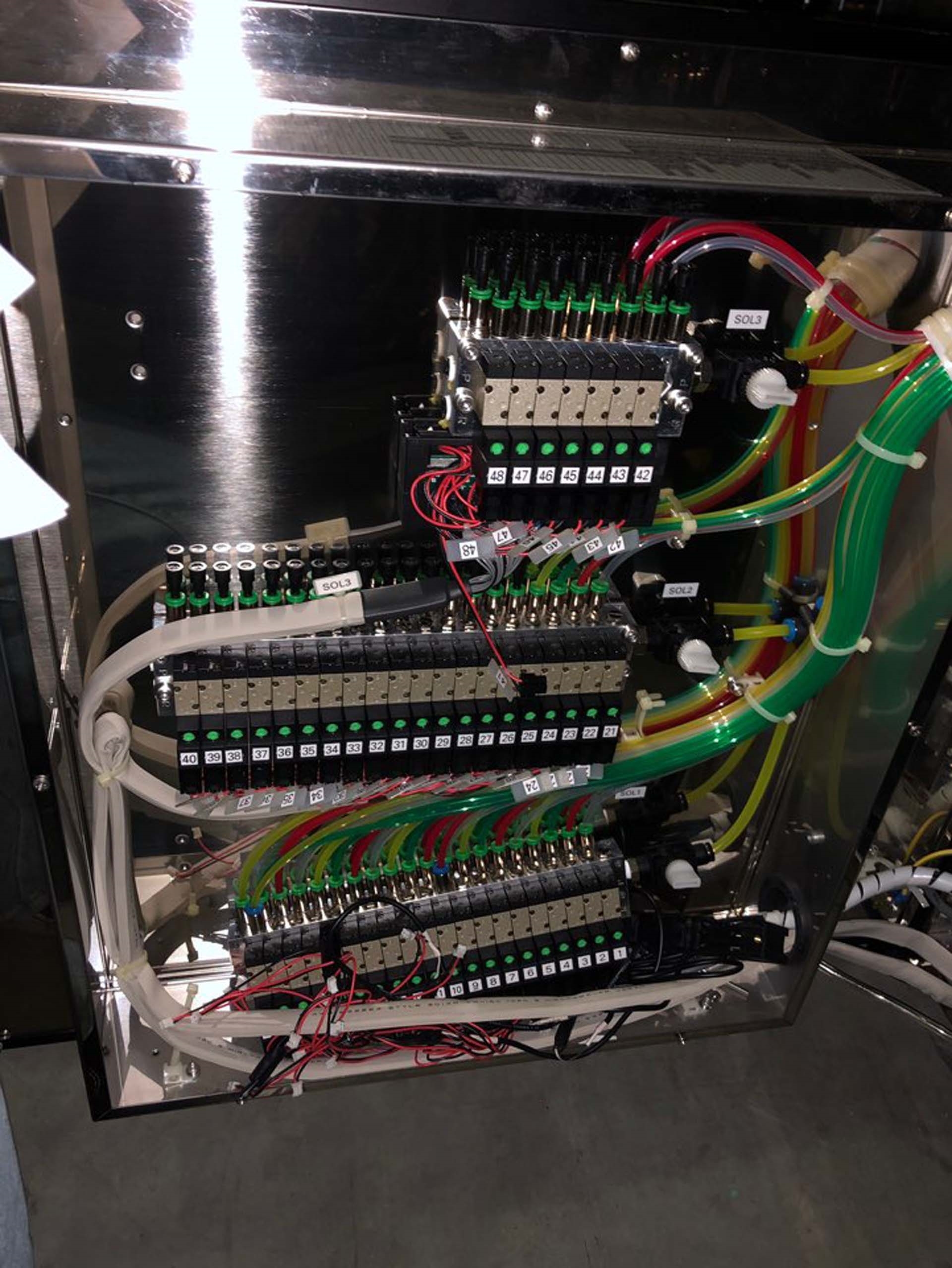

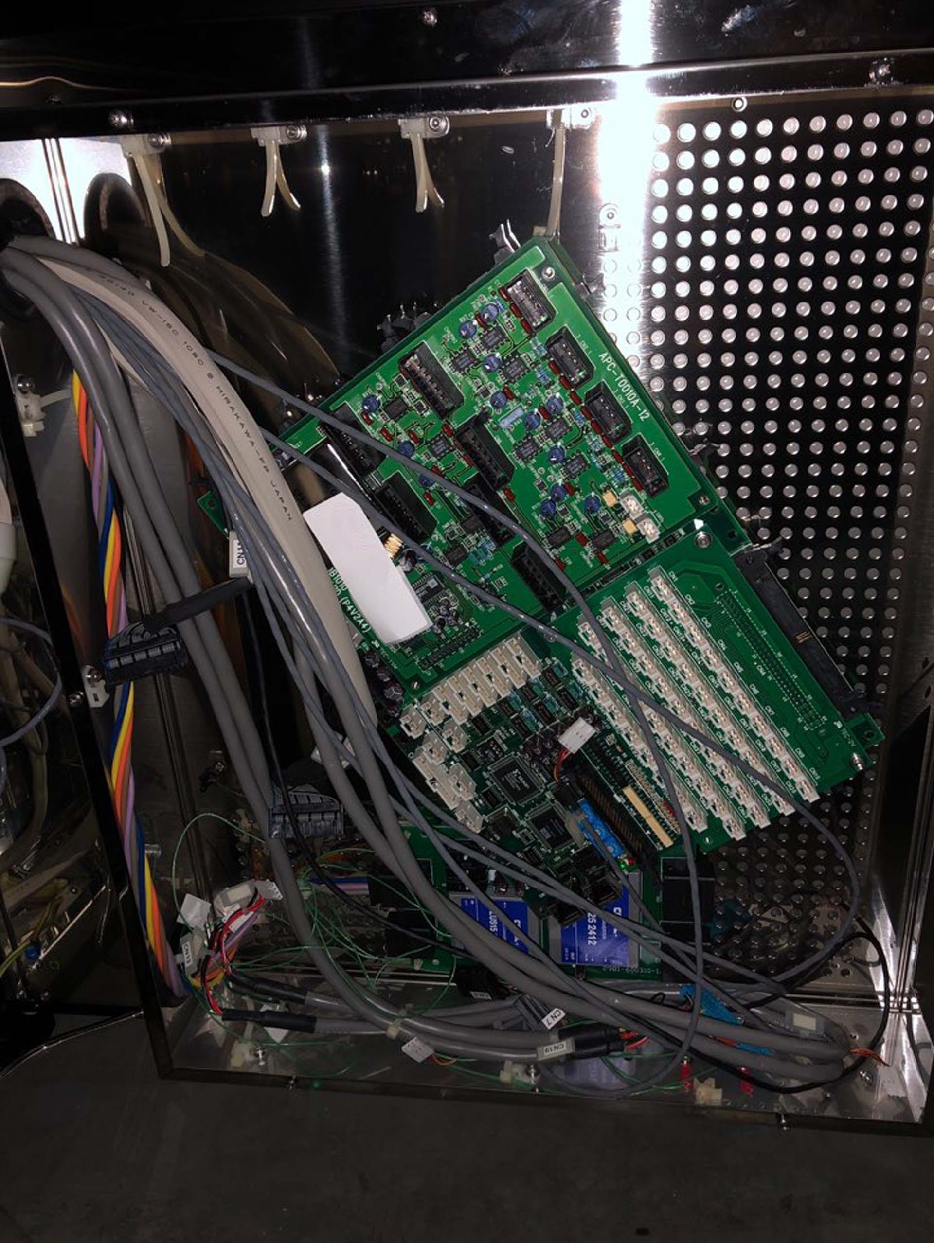

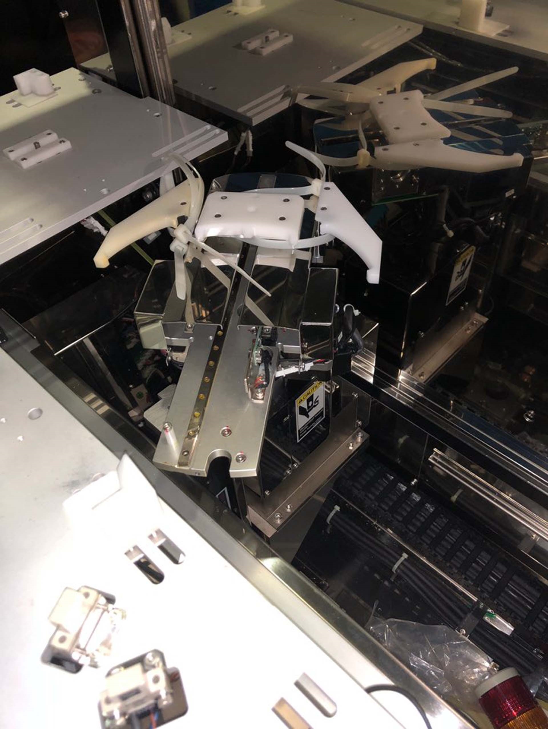

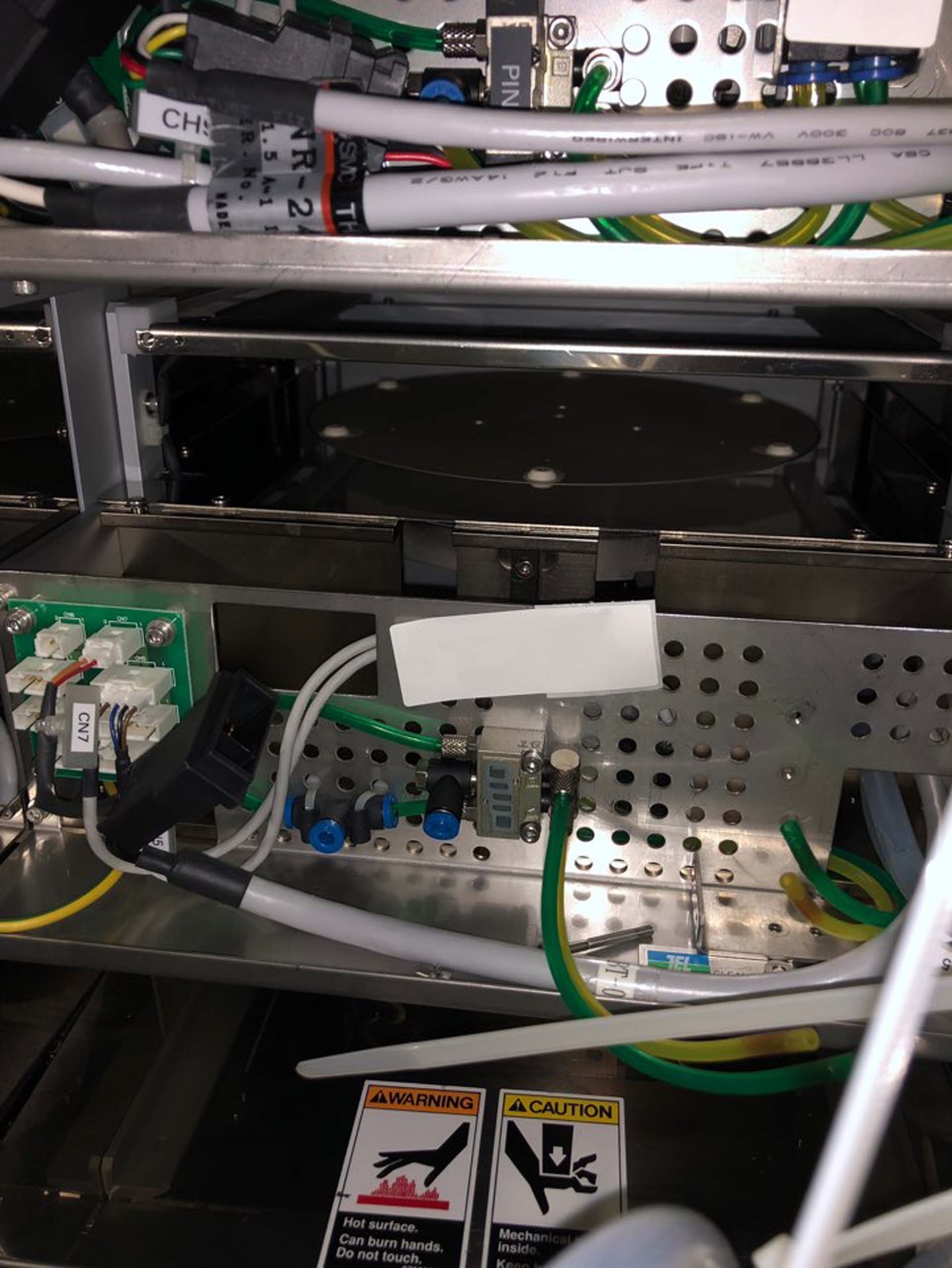

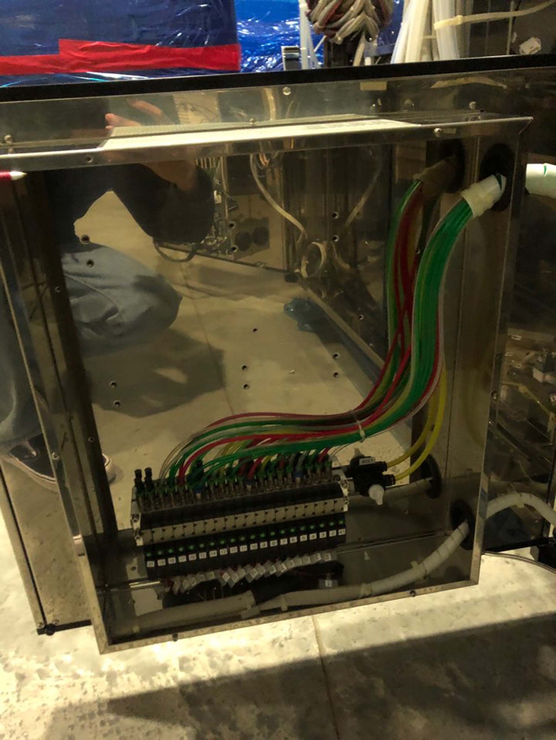

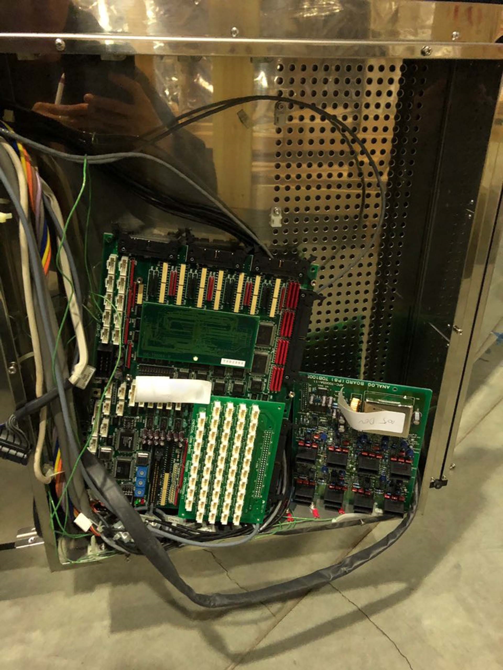

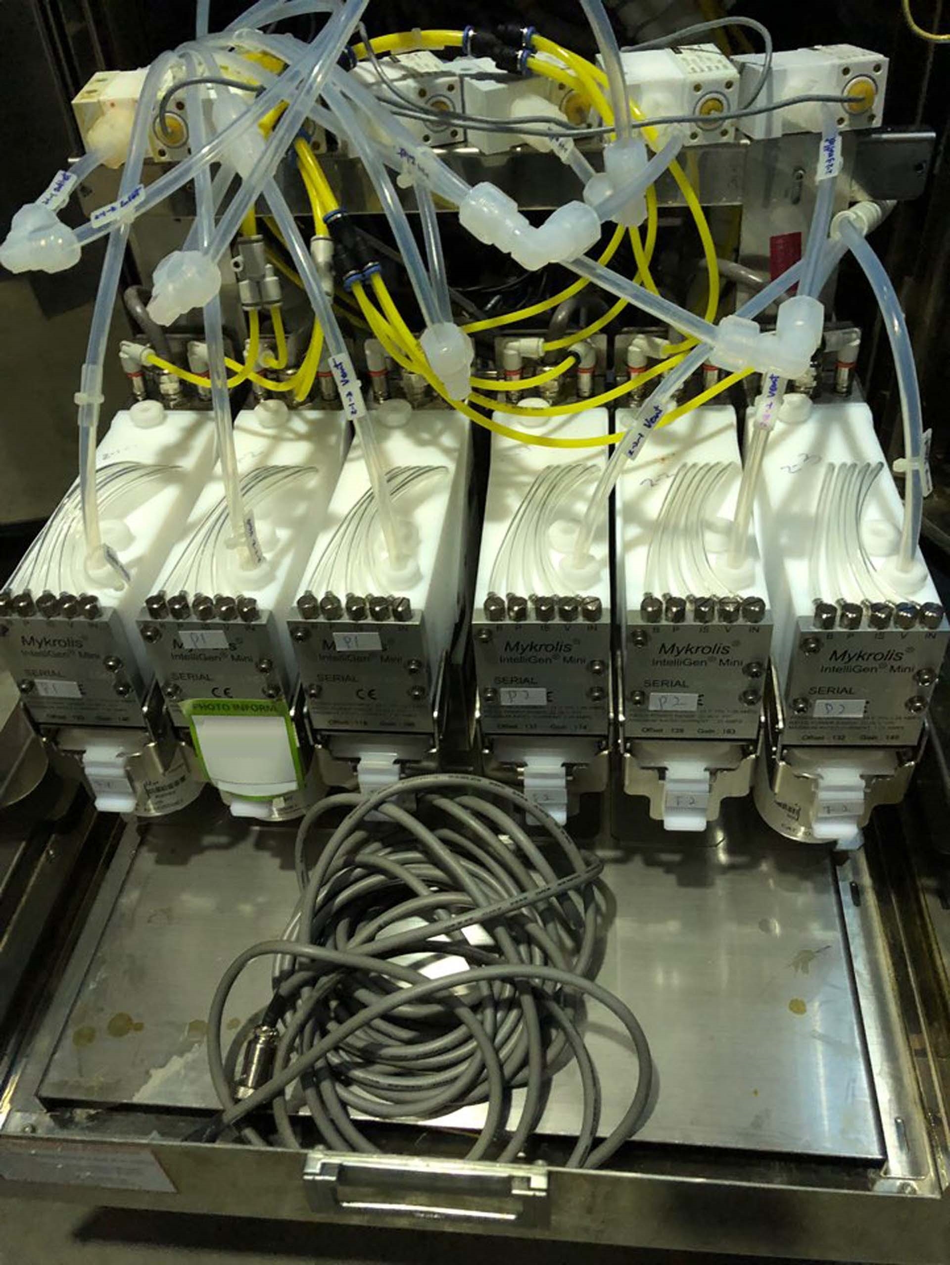

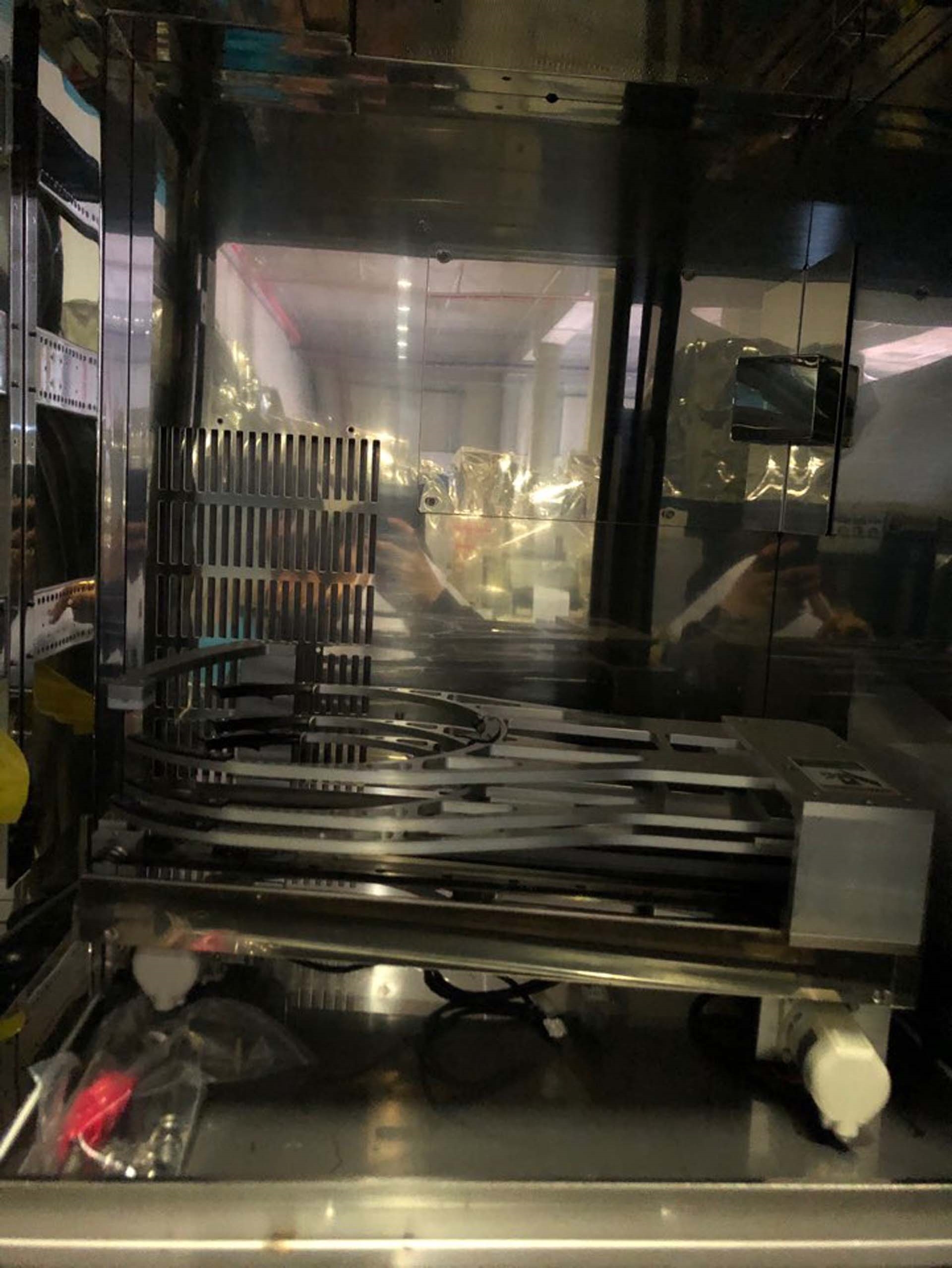

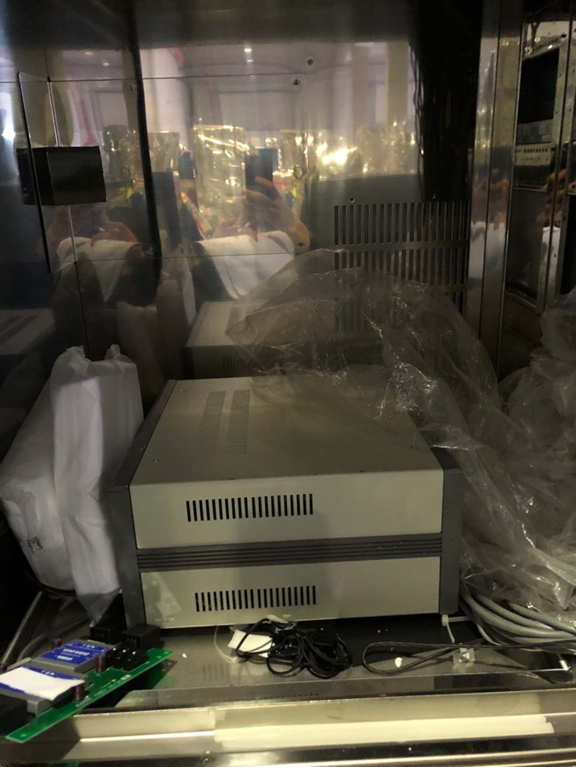

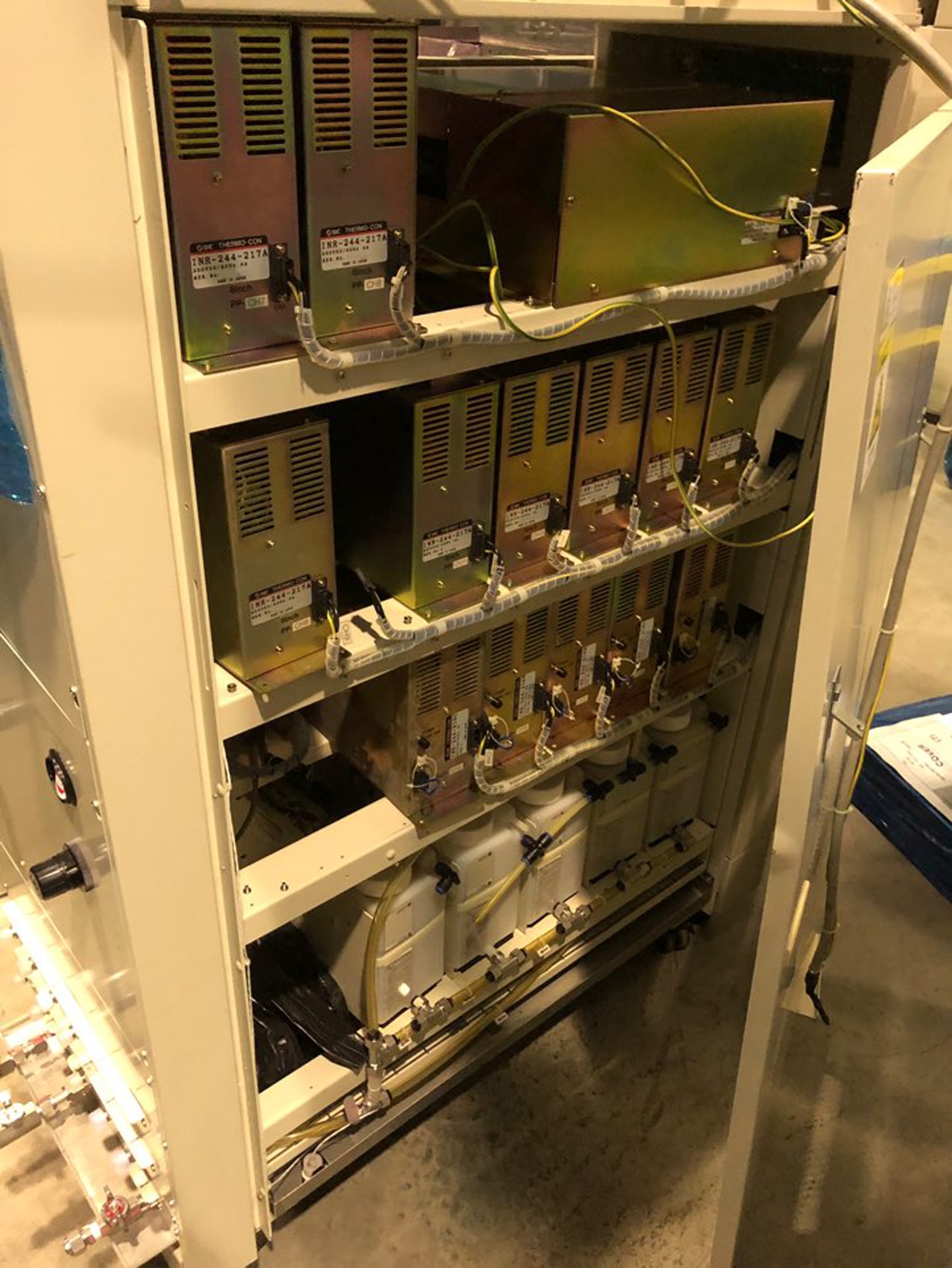

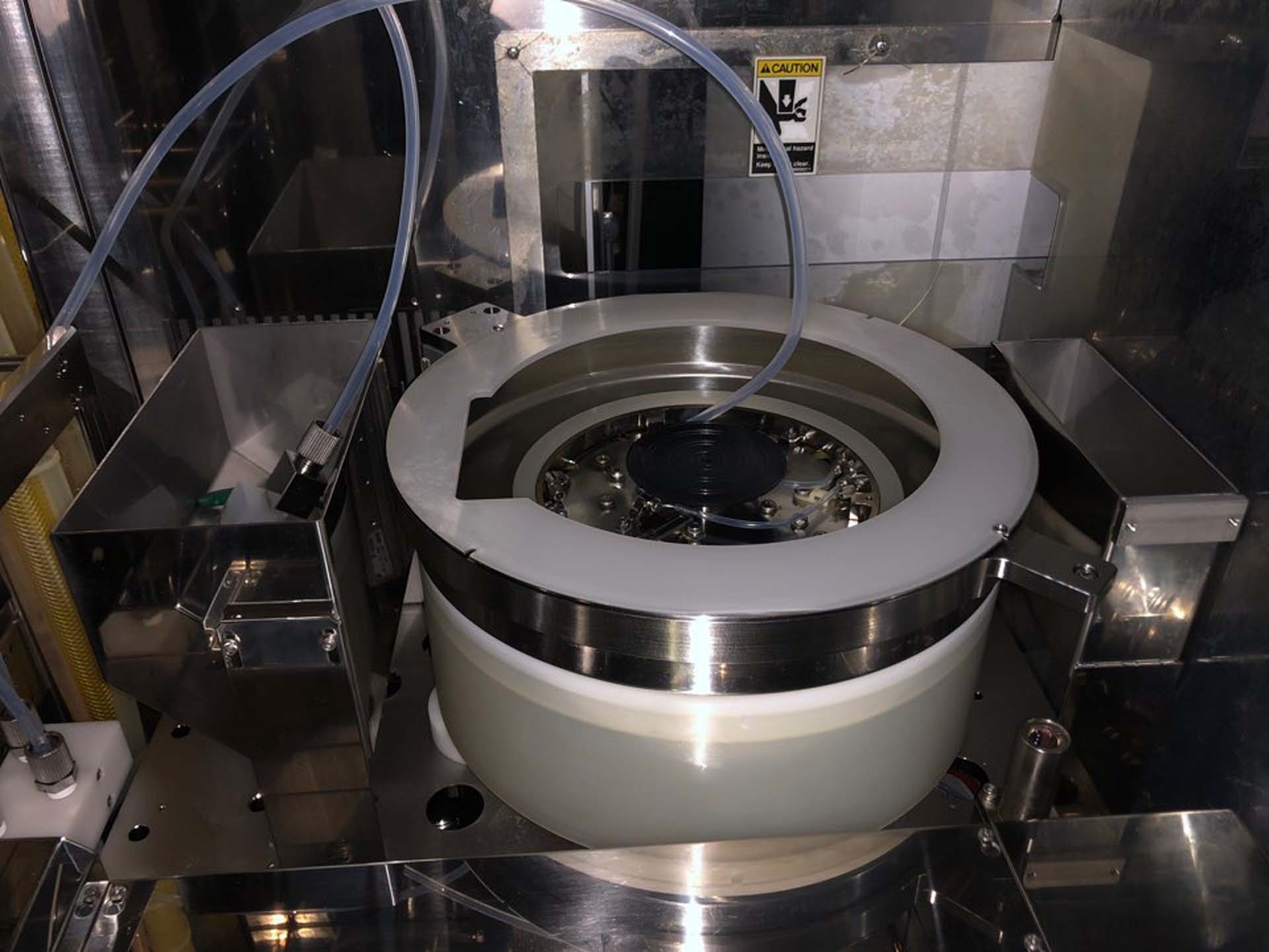

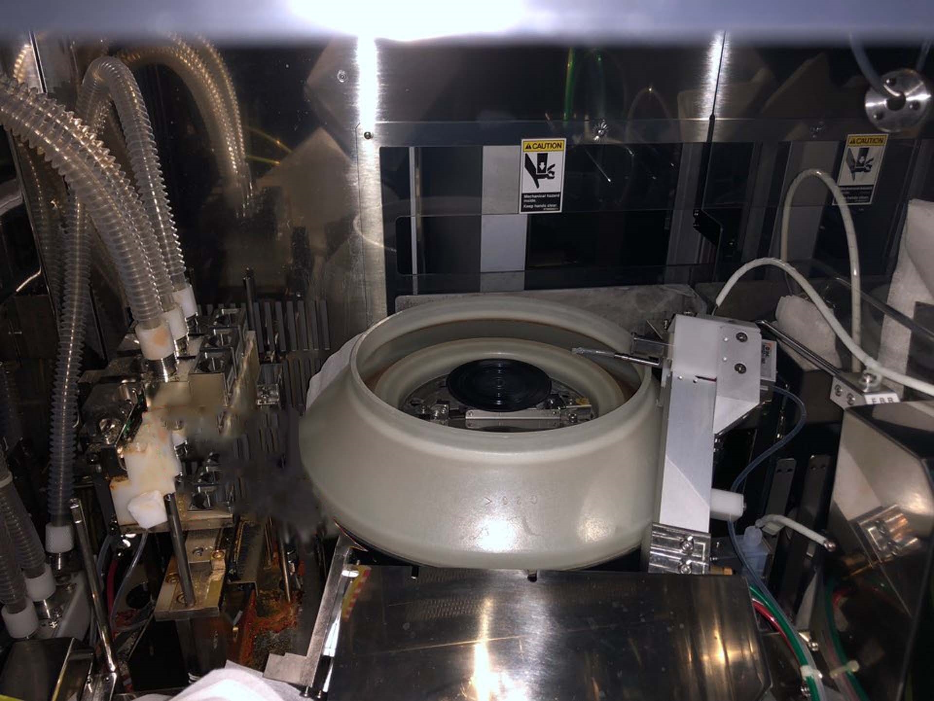

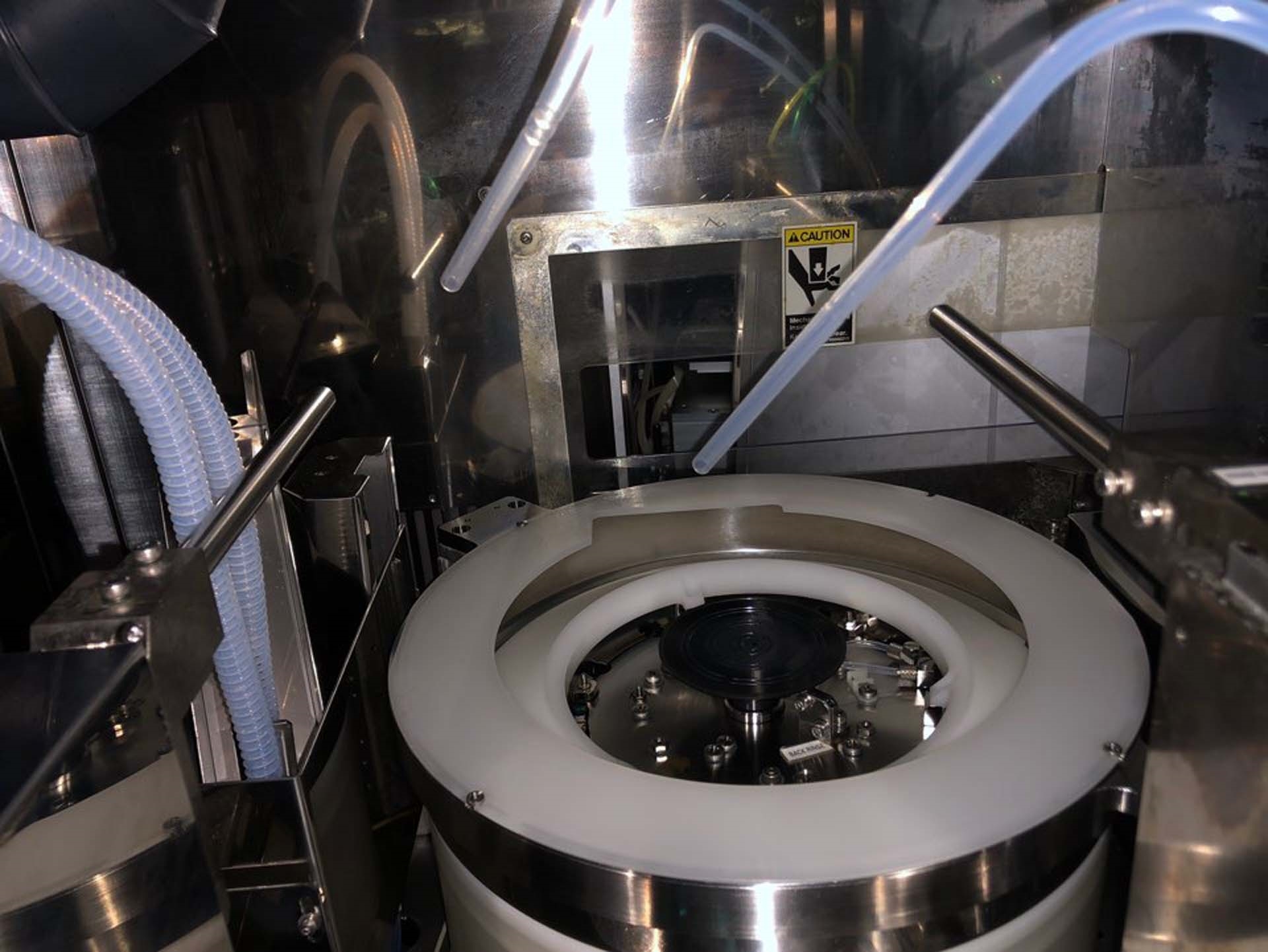

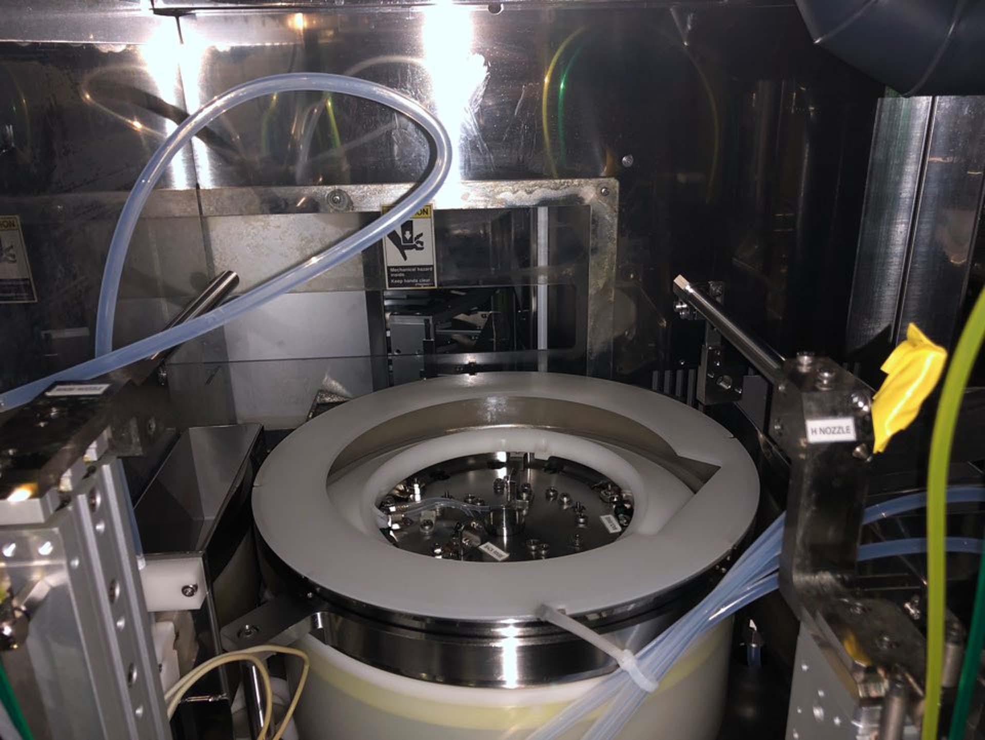

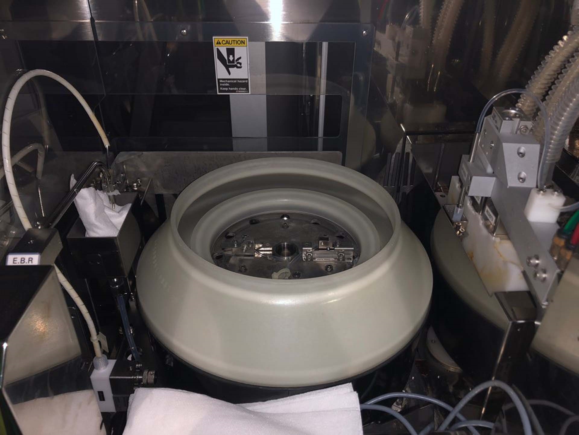


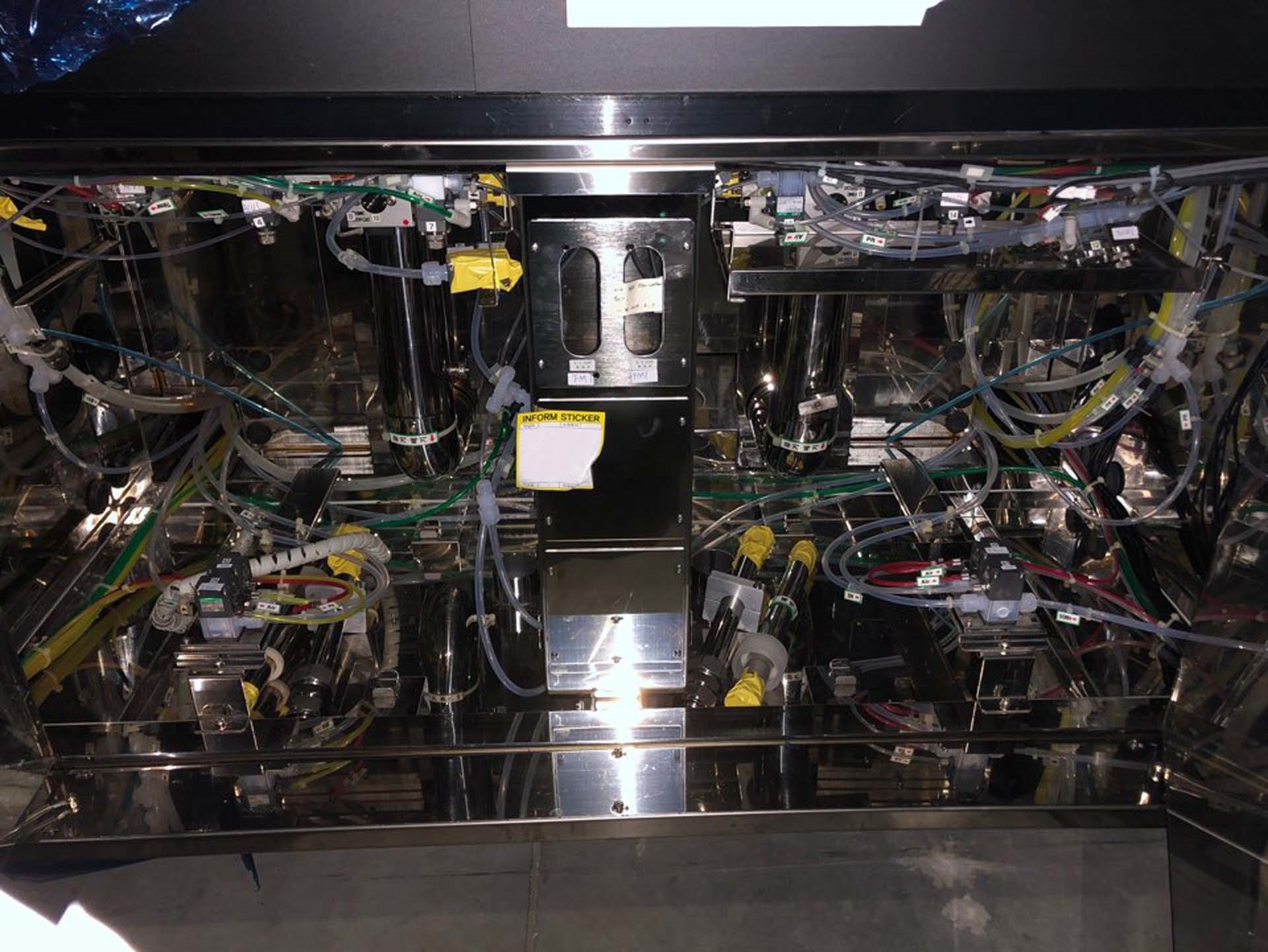

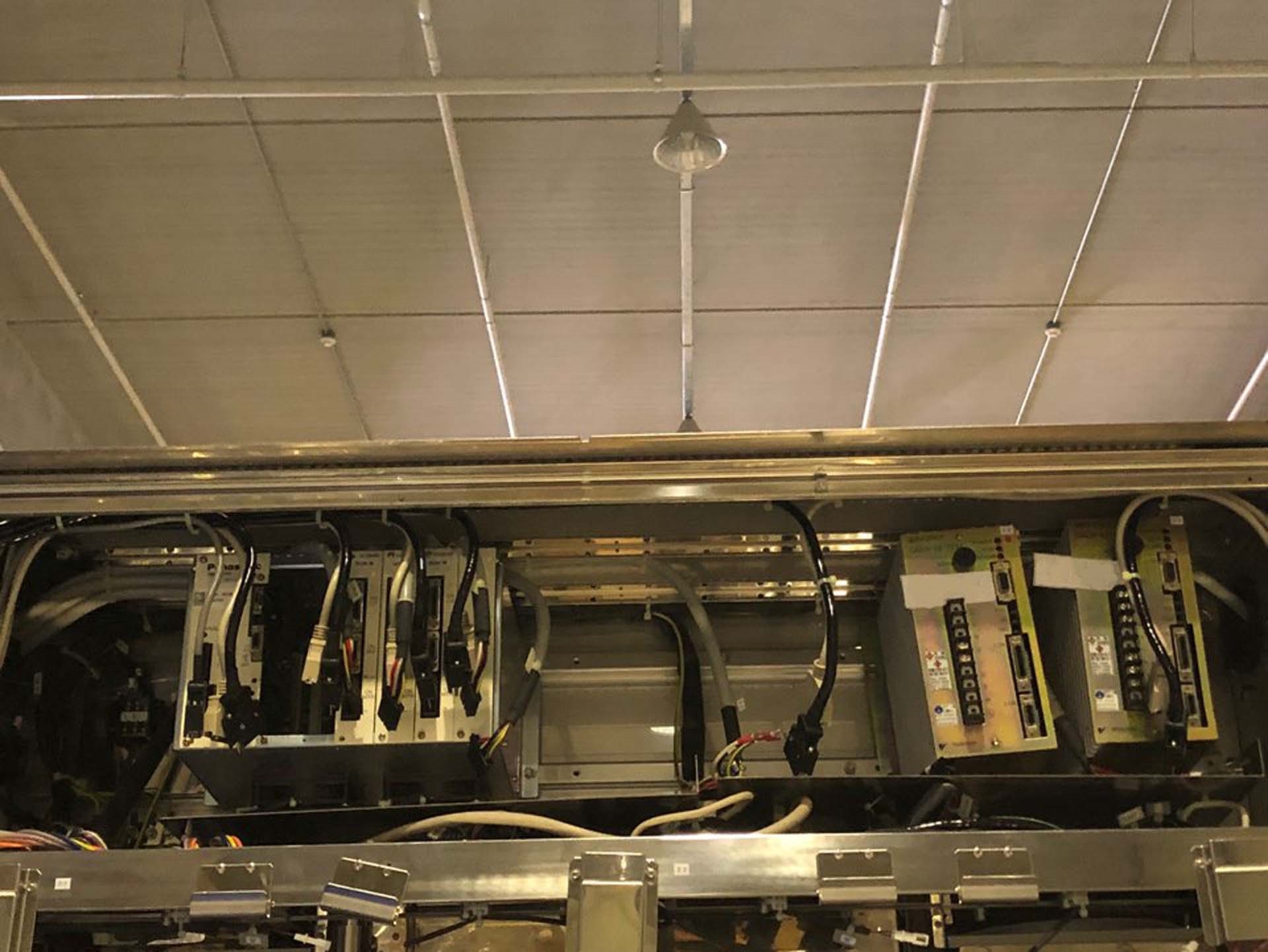

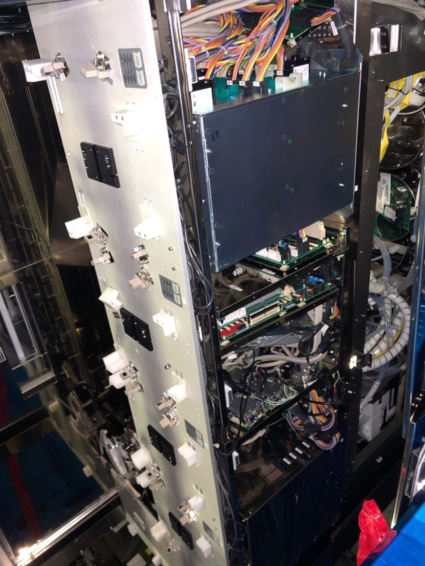


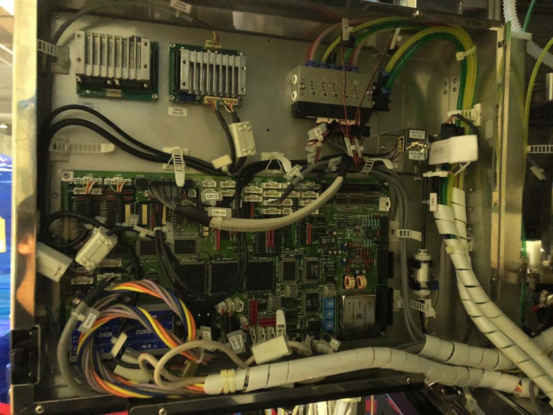

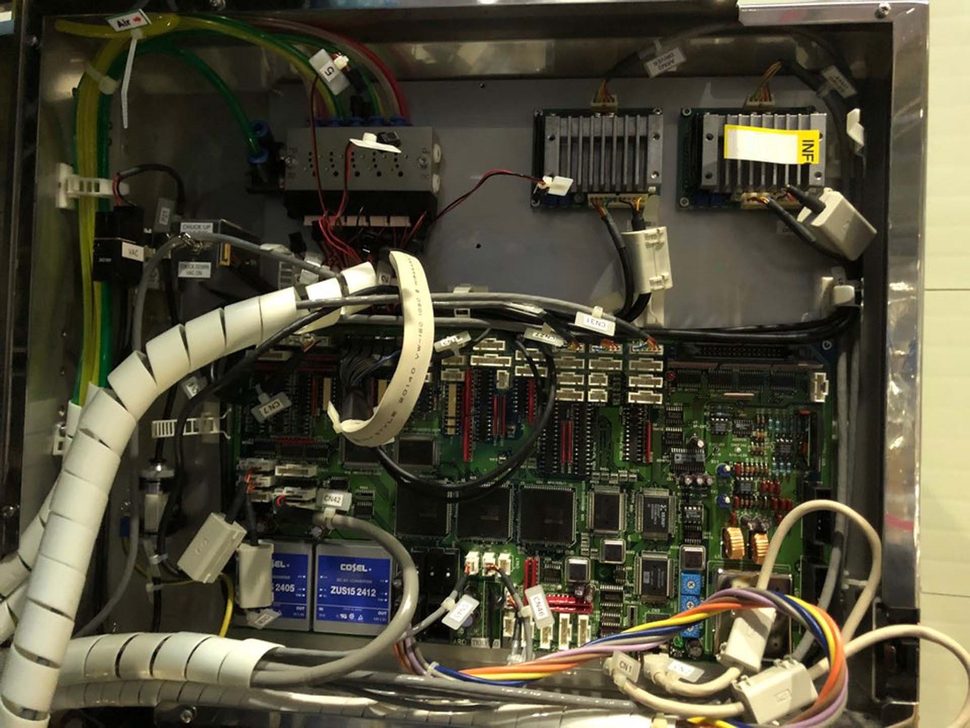

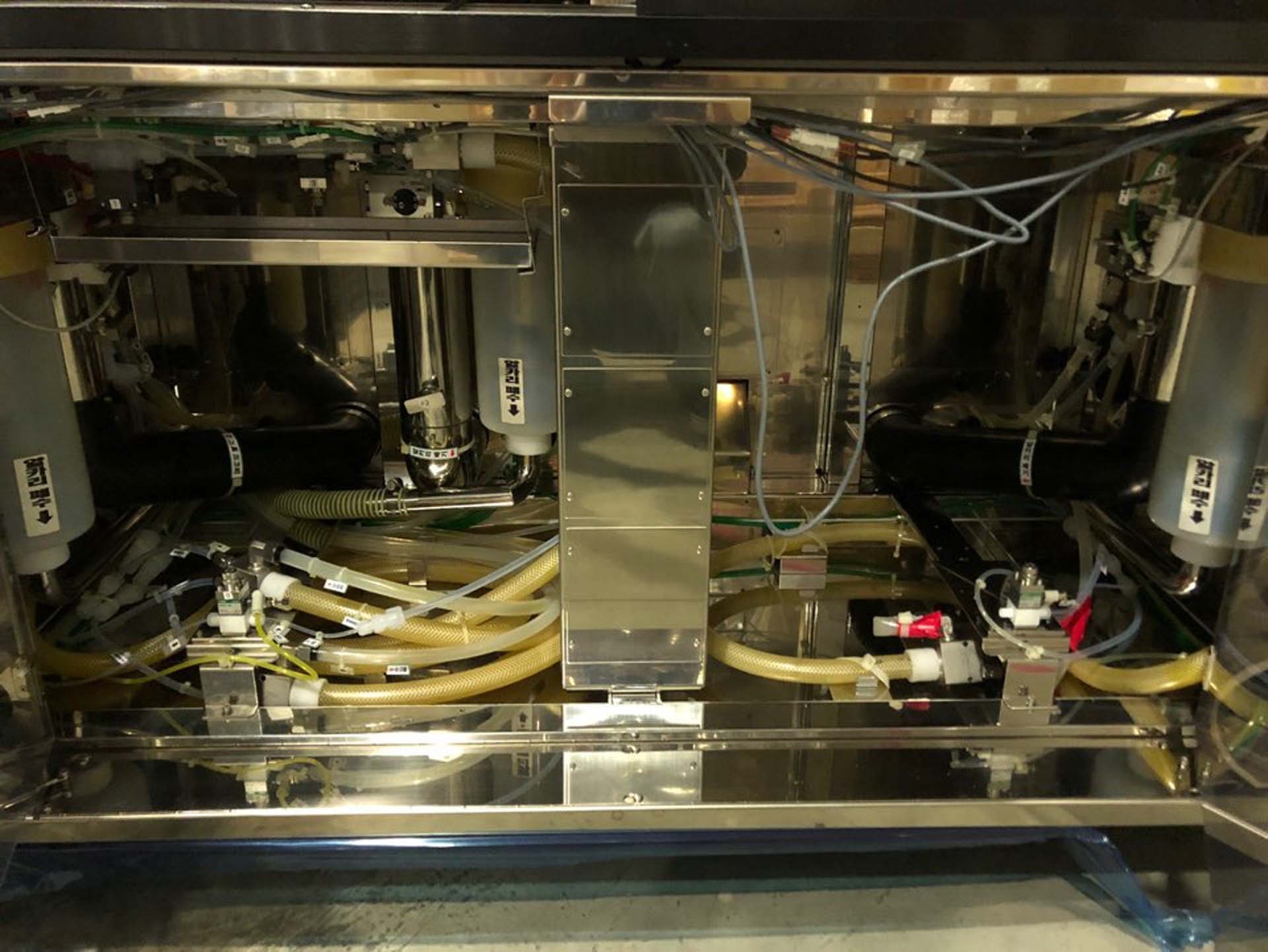


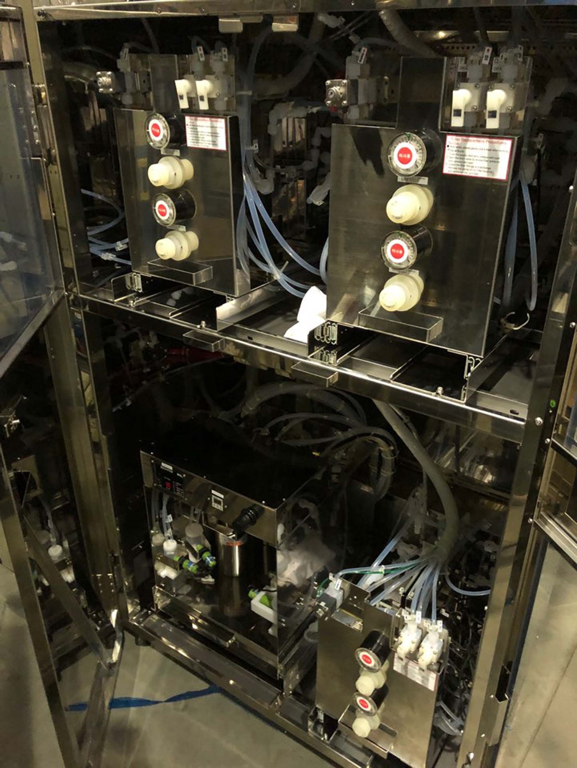

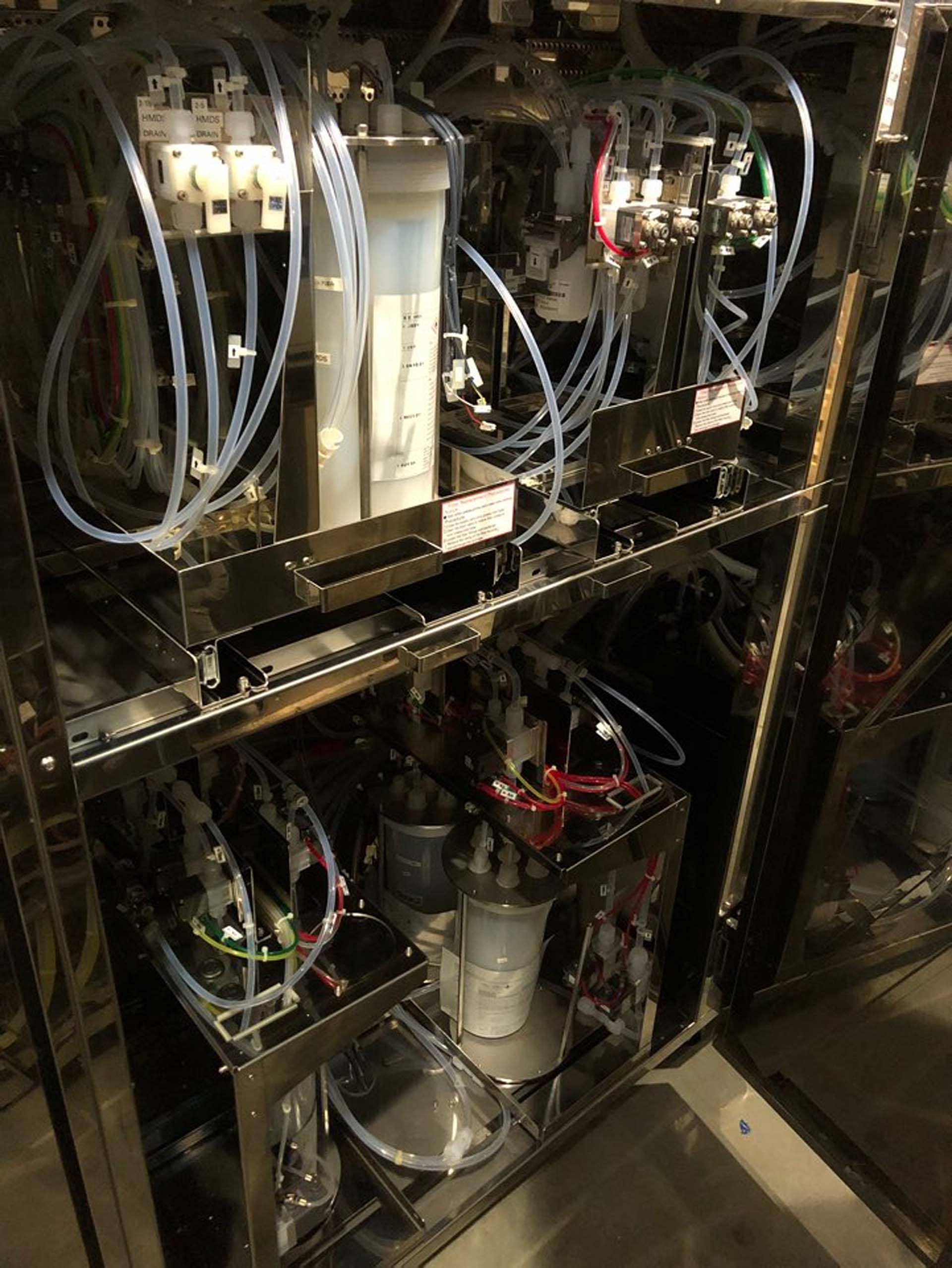

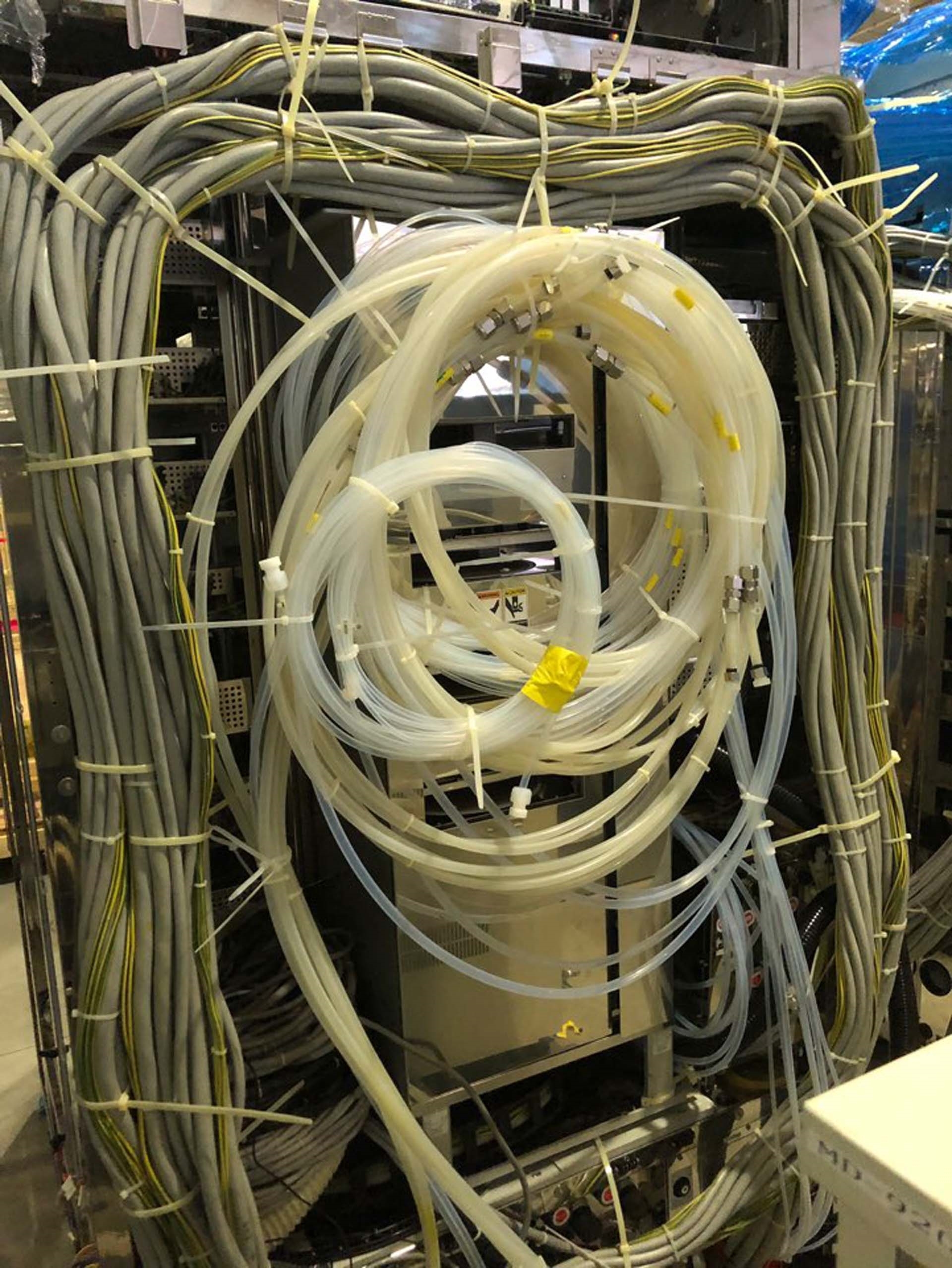

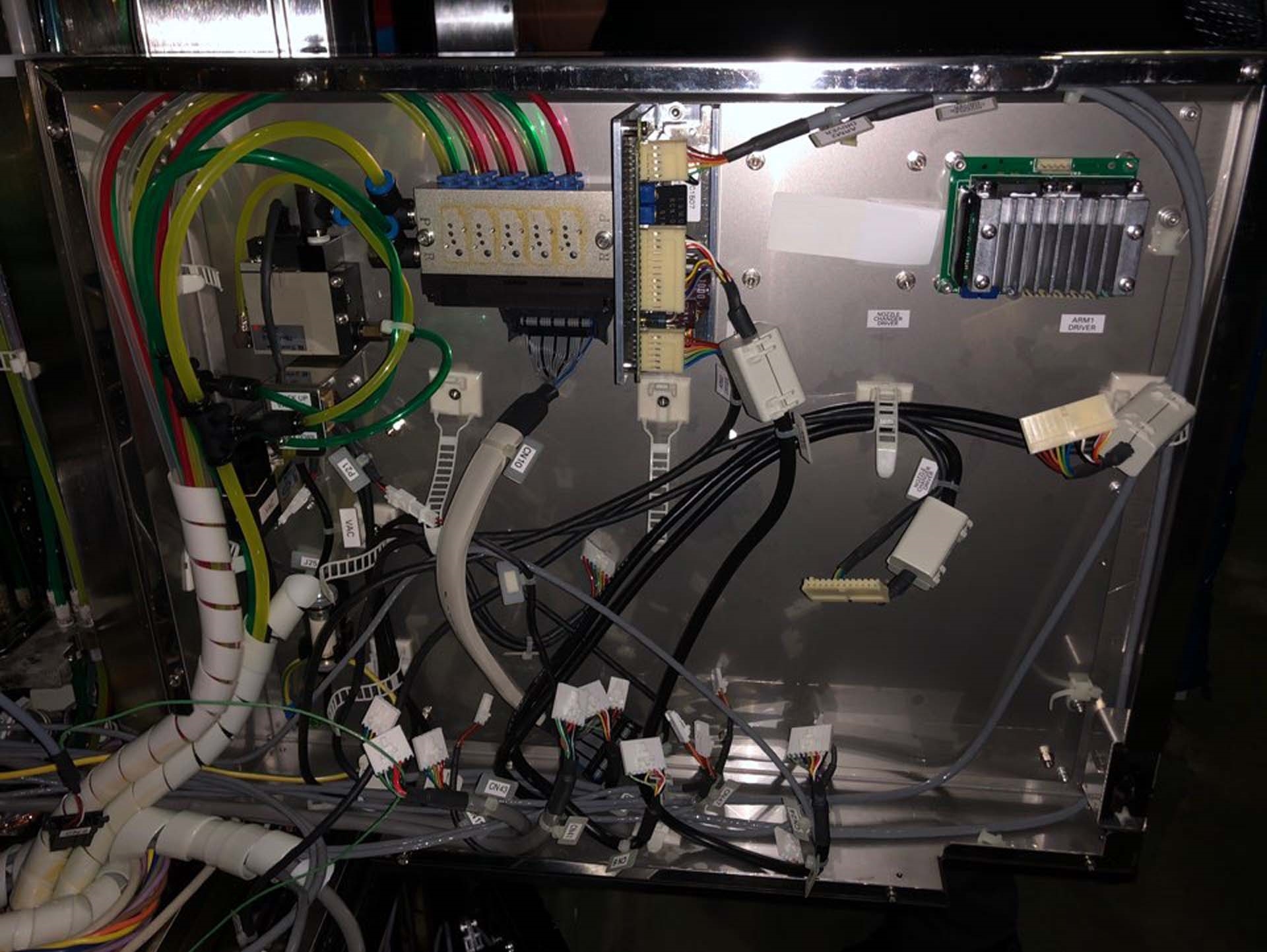

ID: 9241944
Wafer Size: 8"
Vintage: 2000
(2) Coater / (3) Developer system, 8"
Dual block
2000 vintage.
TEL / TOKYO ELECTRON ACT 8 is a photoresist equipment designed by TEL (TOKYO ELECTRON) for photolithography in semiconductor production processes. TEL ACT 8 system enables integrated circuits (ICs) to be produced with improved accuracy and miniaturization. This unit is based on the core technologies of illumination lithography and immersion lithography. The enhanced illumination technologies of TOKYO ELECTRON ACT 8 machine reduce the effect of diffraction and distortion, allowing for optimal patterning of complex ICs with improved precision. Its immersion lithography capabilities enable extremely small pitches. This is attained by utilizing a low numerical aperture (NA) projection lens and radiation source. This allows for precise patterning and high-resolution printing on semiconductor wafers. The tool also comes with an advanced anti-reflection technology, reducing unwanted light reflections that can contaminate the wafer and end product. TOKYO ELECTRON ACT 8 asset also features a built-in Dark Substrate (DS) Inspection Model, which inspects for any defects on the wafer before or during the lithography process. This gives the user precise real-time information on the wafer's condition, greatly improving the reliability of the final product. The equipment also comes with a Mark Alignment System (MAS) for accurate chip placement on the wafer. Furthermore, the pattern correction software included in the unit ensures each chip is placed in the right location during production. ACT 8 machine's CCD camera enables monitoring of the entire lithography printing process. This helps in monitoring any unexpected changes in the pattern while the process is ongoing, allowing for corrections to be made before the wafer is damaged. The tool also has a Position Detection Security (PDS) asset to help prevent unauthorized personnel from accessing the model. TEL ACT 8 photoresist equipment is one of the most advanced photolithography systems currently available for use in IC production. It provides an excellent balance of both illumination and immersion lithography technologies, allowing for the producing of highly complex ICs with utmost precision. The DS inspection and MAS also help with ensuring that the chip placement and wafer quality is maintained throughout the manufacturing process.
There are no reviews yet


