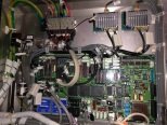
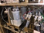
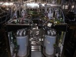
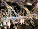
Used TEL / TOKYO ELECTRON ACT 8 #9244824 for sale
URL successfully copied!
Tap to zoom
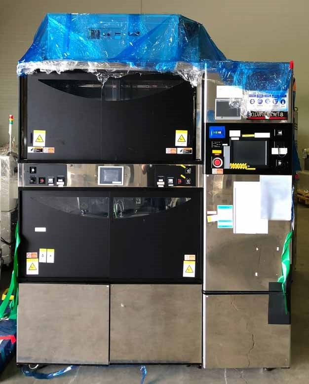

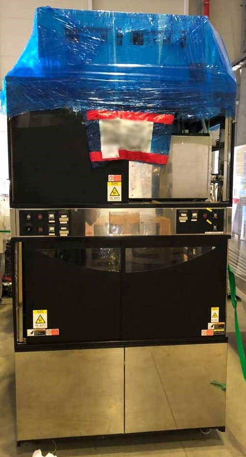

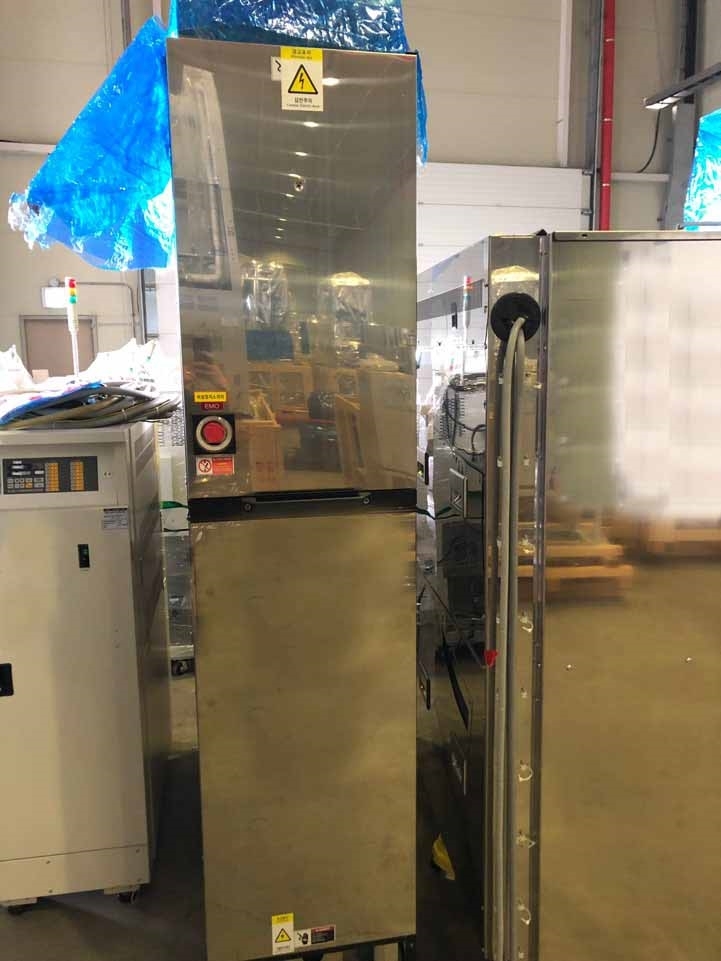

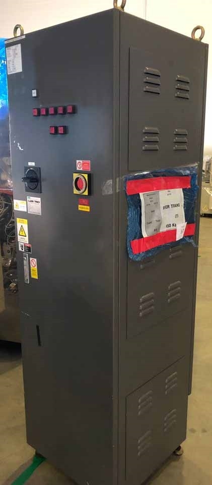

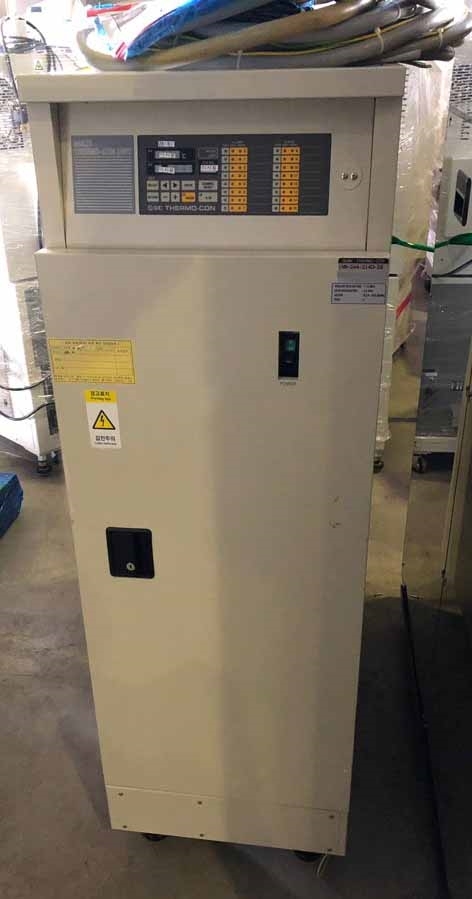


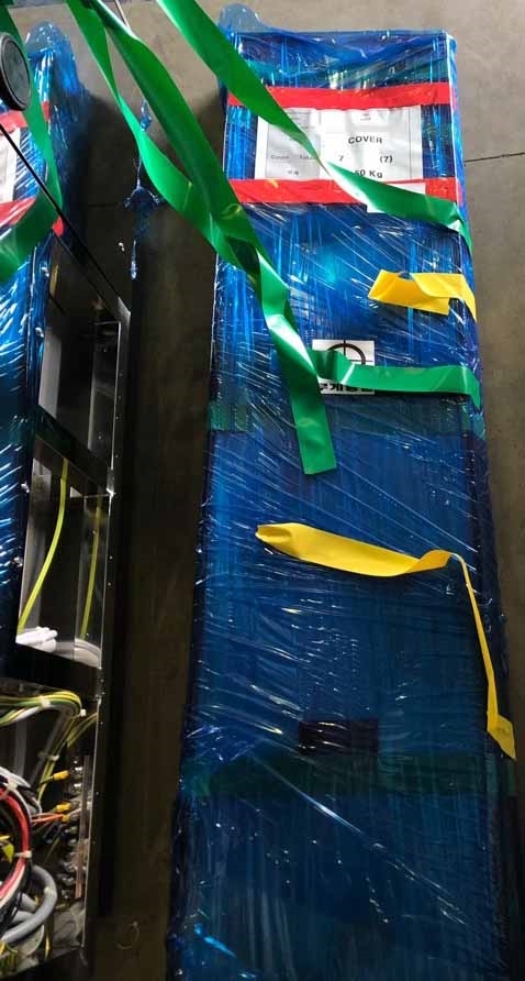

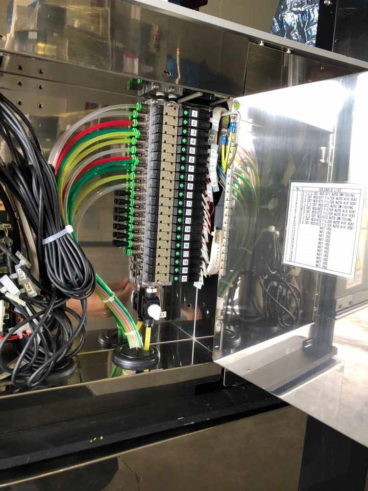

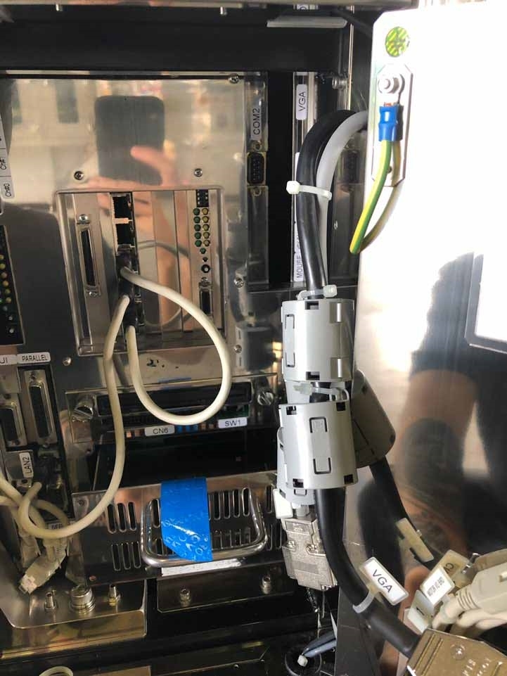

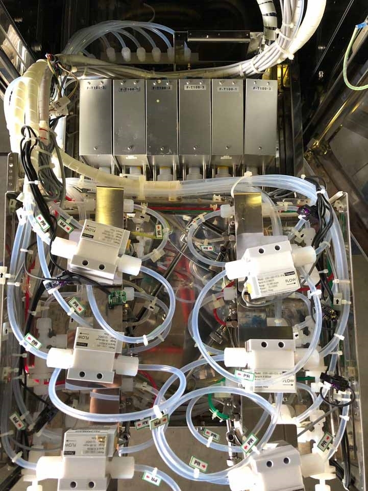

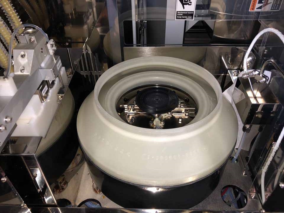

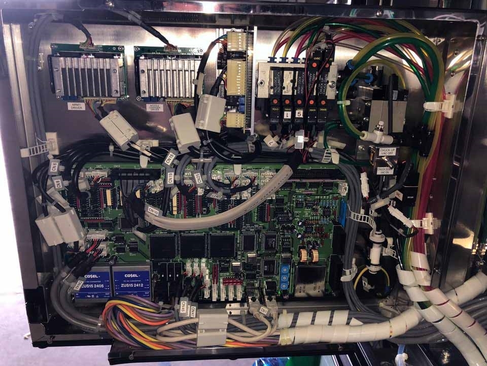

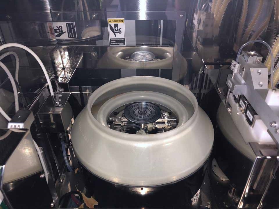

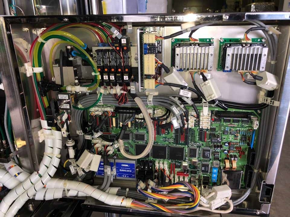

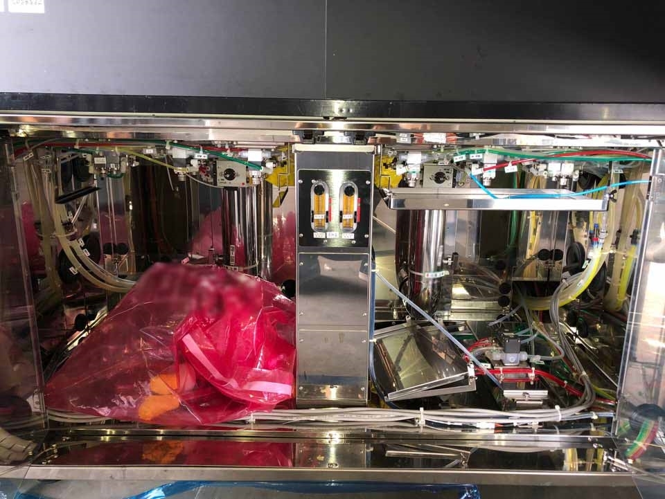

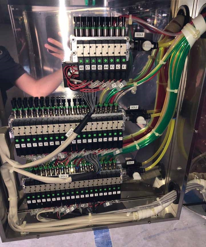

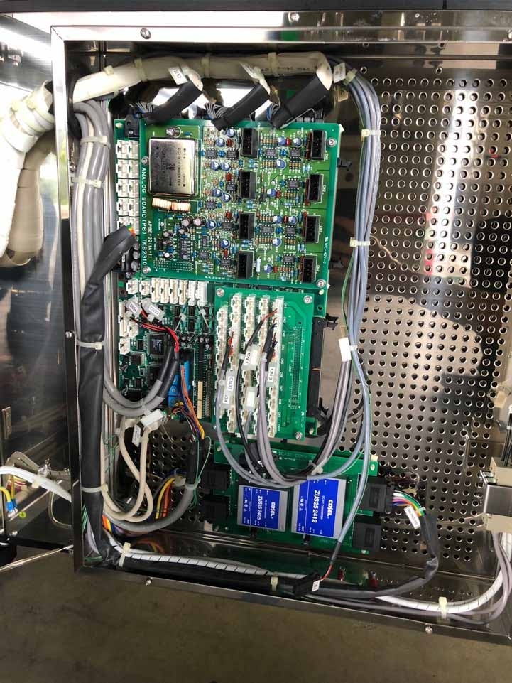

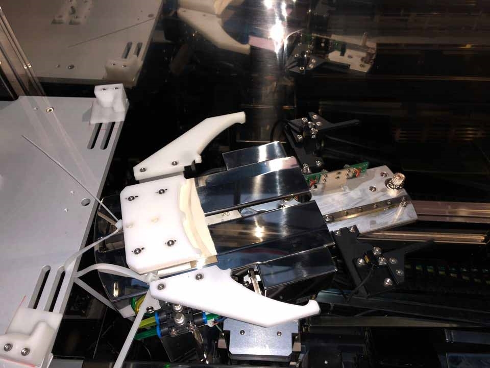

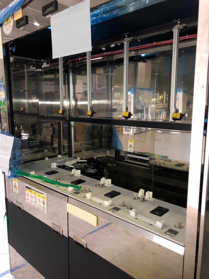

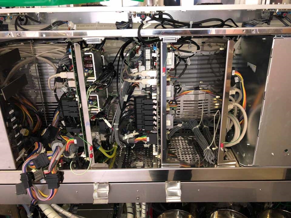


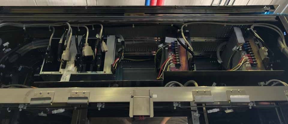

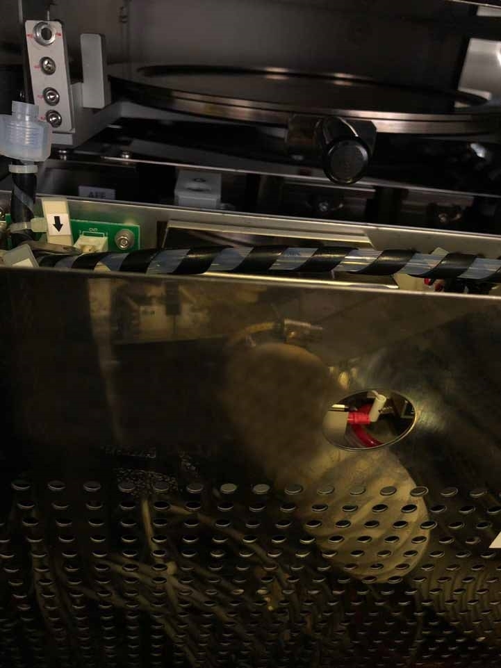

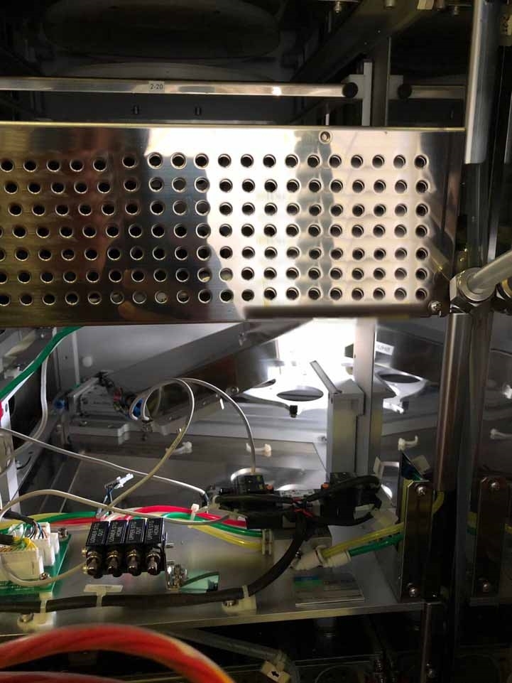


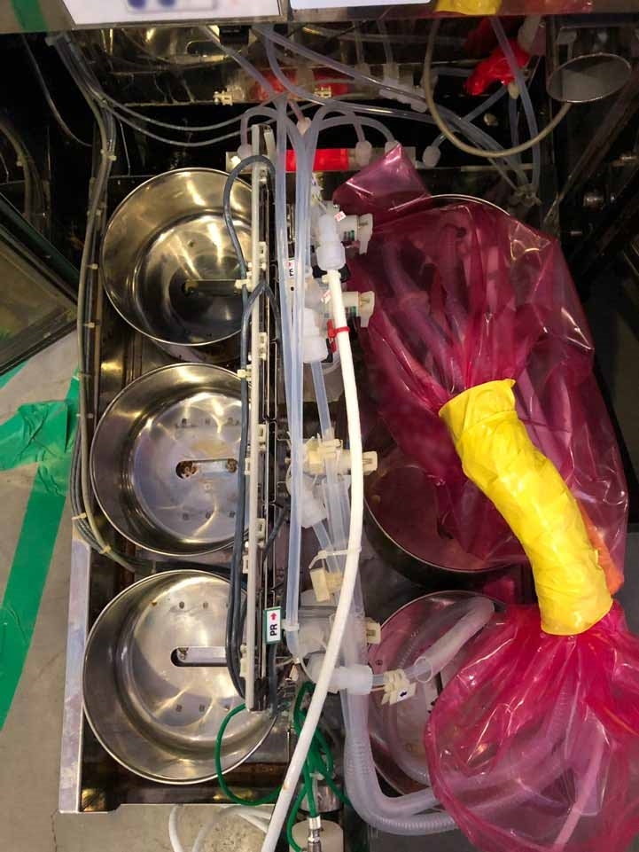


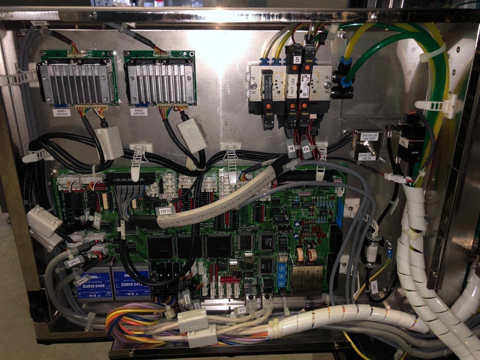

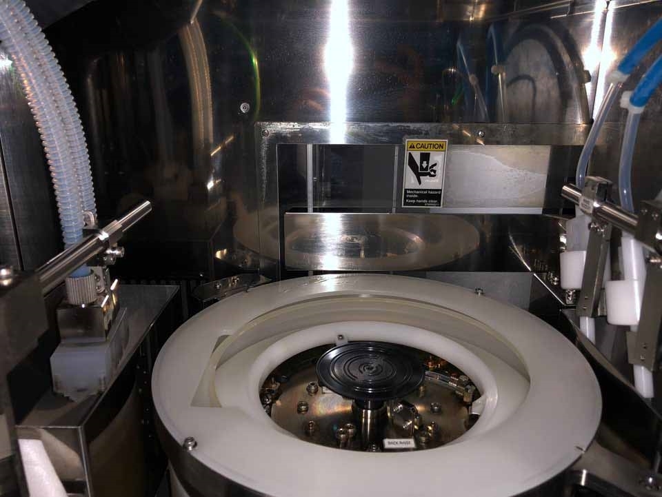


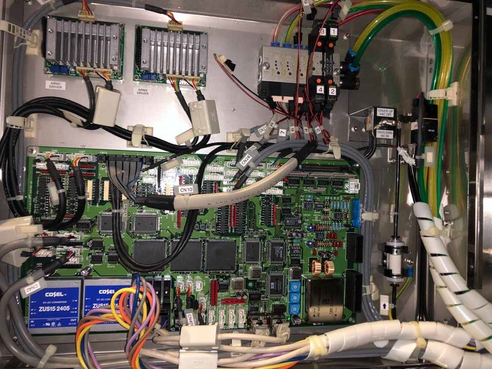

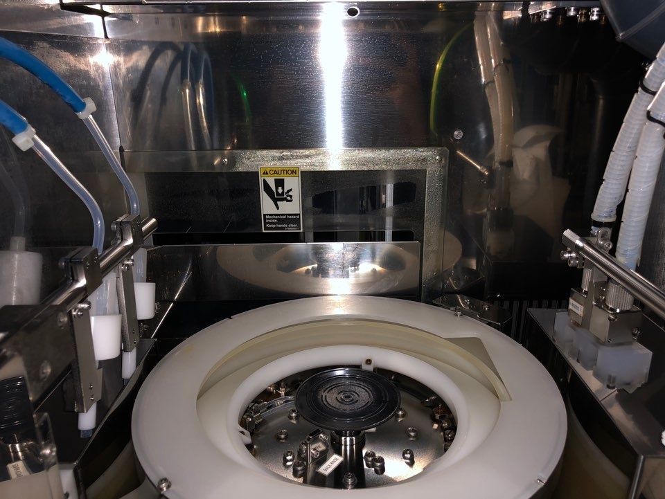


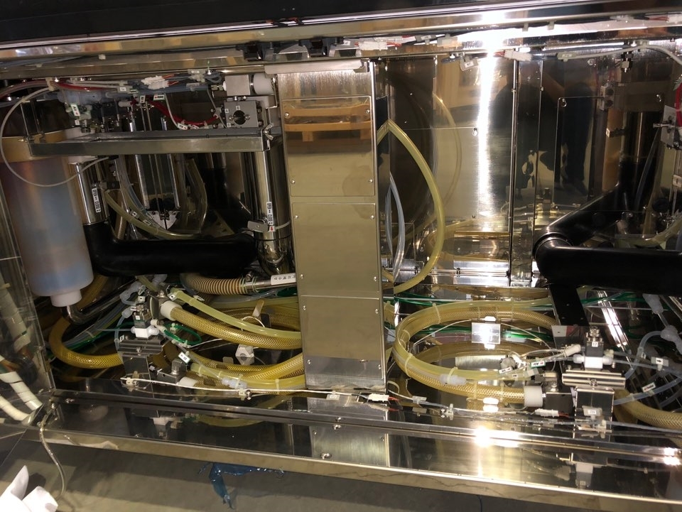

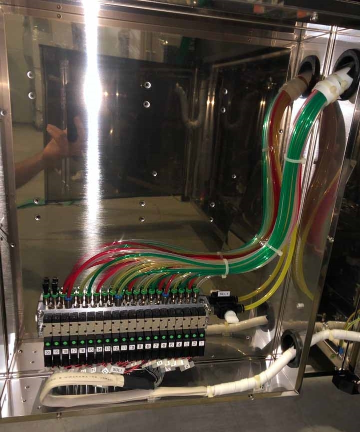

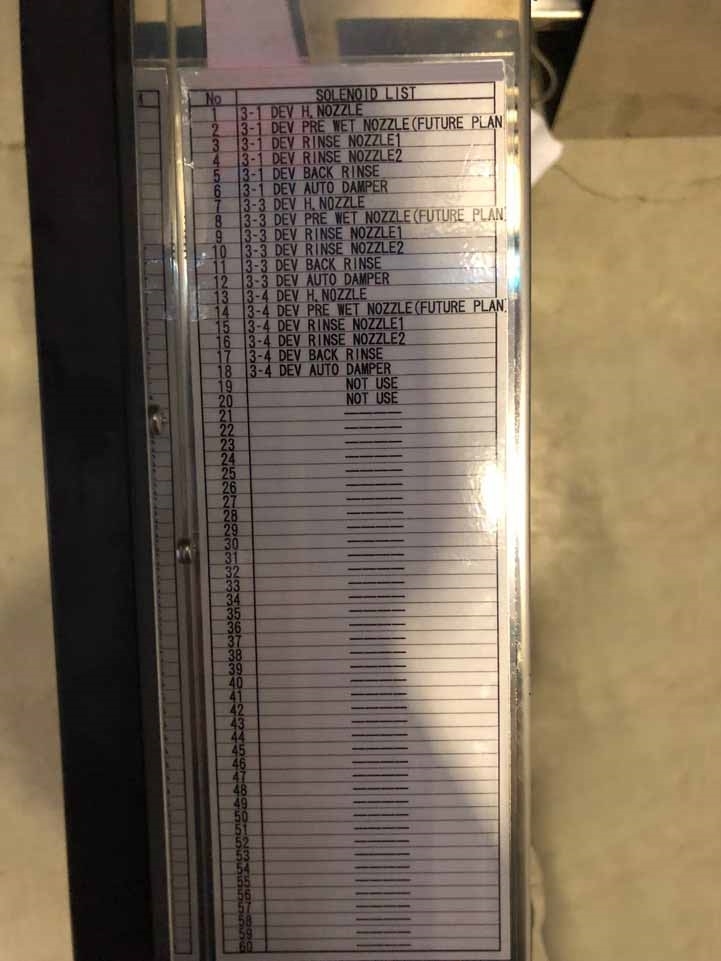


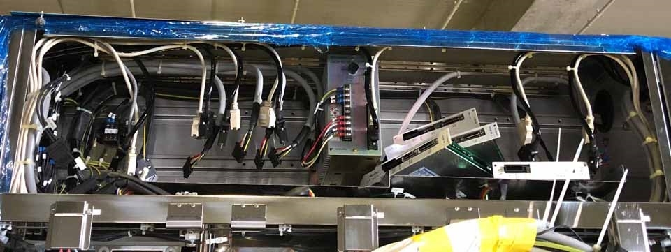

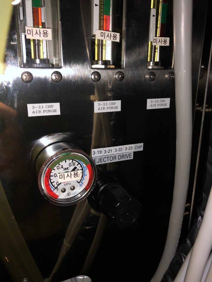


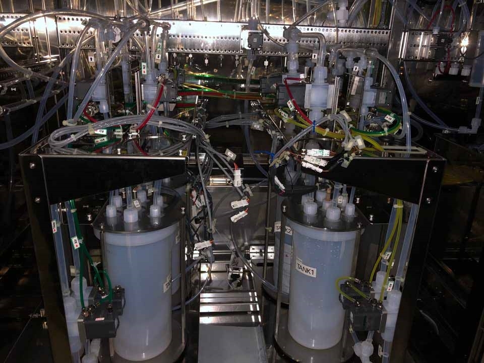

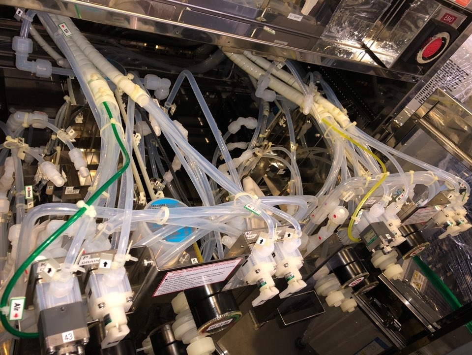

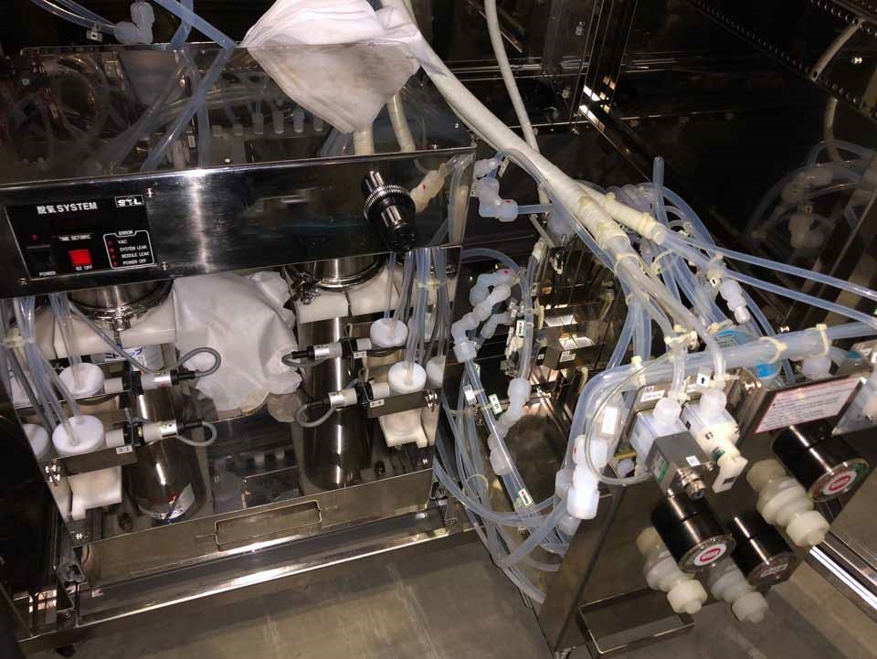

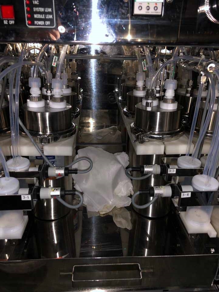

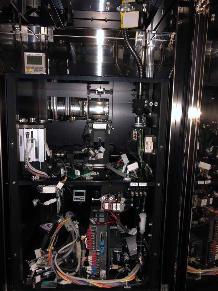


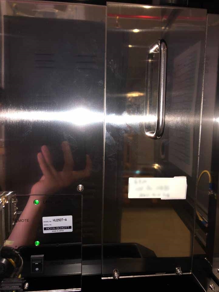

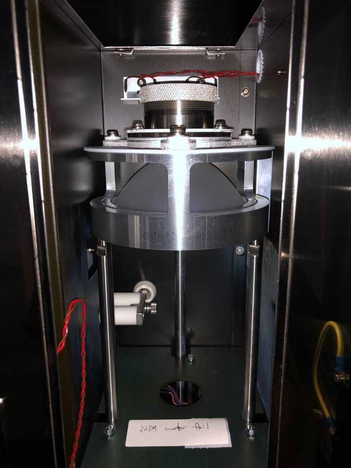

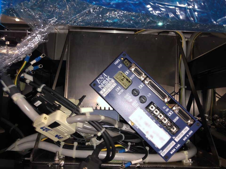

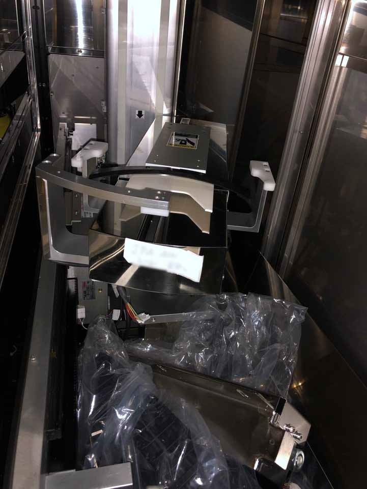

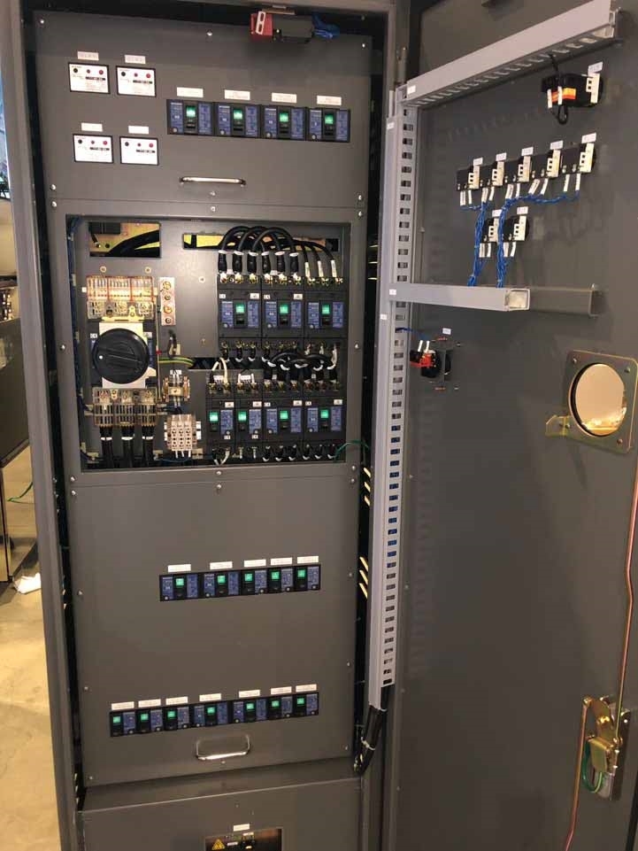

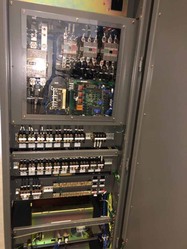

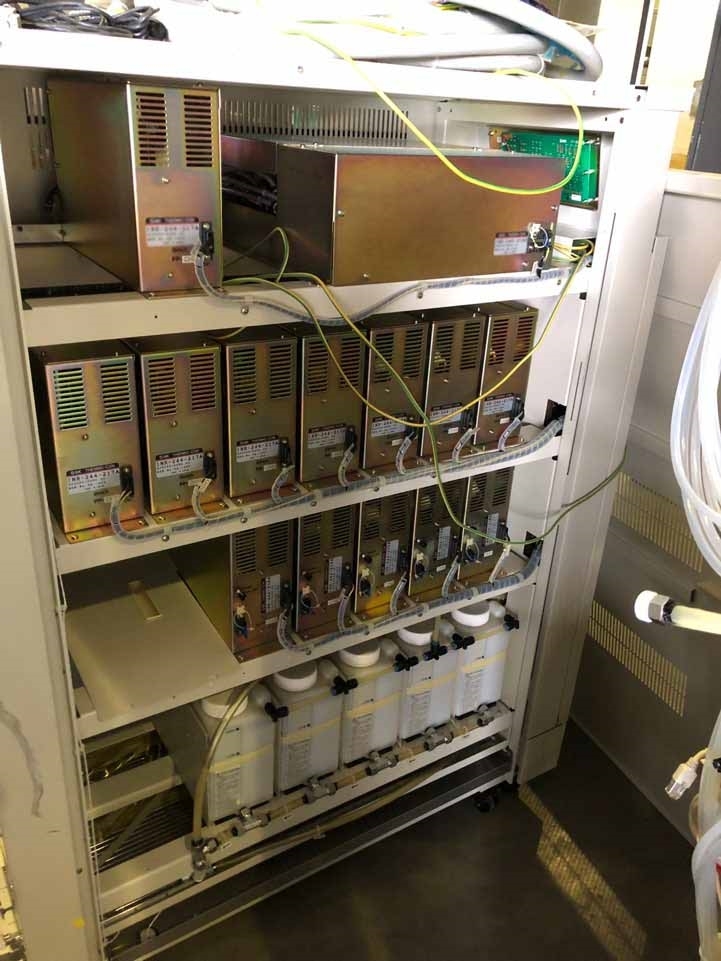

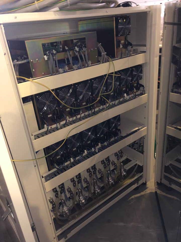

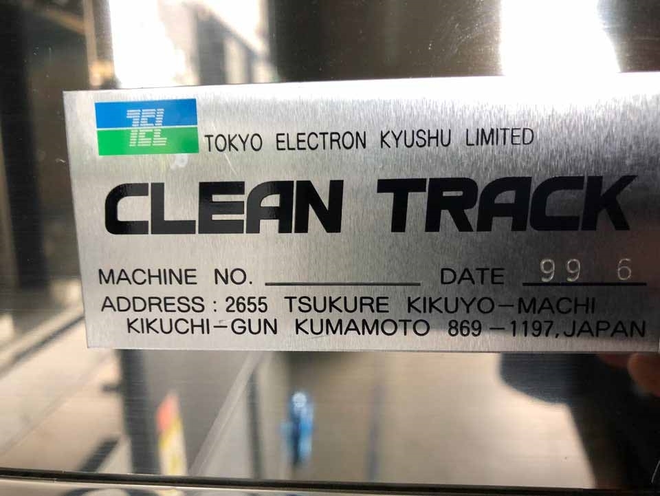

TEL / TOKYO ELECTRON ACT 8 is a photoresist equipment designed for advanced lithography. This system provides researchers and industry professionals with high resolution, reproducible and robust patterning capabilities for developing electronic circuits in advanced semiconductor wafer technologies. The unit is based on a self-aligning, multi-layer resist technology that enables high-resolution patterning of nanoparticles with total control of the geometry and size of the patterns. The resist machine is comprised of a deep ultraviolet (DUV) light source and a resist formulation that is tailored for optimal patterning performance. The deep UV light source allows for highly accurate and efficient patterning of the resist layers with a wide range of exposures. The resist formulation is engineered to provide precise control of the pattern dimensions and its lithographic characteristics, enabling excellent pattern fidelity and repeatability. These features provide the tool with high productivity and uniformity, making it an ideal choice for critical application areas such as high performance memory and image sensors. The asset supports mixed layer lithography, which allows designers to combine several layers of positive and negative resists to precisely control the patterns dimensions and other critical parameters in production. Additionally, the model features advanced auto-focus and auto-exposure capabilities with pre-programmed process parameters for repeatable and accurate results. TEL ACT 8 equipment is equipped with an intuitive interface and user friendly controls which provide users with convenient and precise access to all the process parameters. It also comes with comprehensive documentation and extensive application support. The system is compatible with a wide range of etching and deposition processes and also supports multi-project wafer capability. TOKYO ELECTRON ACT 8 is a versatile and effective photoresist unit that offers users superior performance and repeatability for advanced lithography. It provides excellent pattern control with advanced auto-focus and exposure capabilities, as well as reliable process fidelity even with demanding applications. Its comprehensive support and user friendly interface make it an ideal choice for research laboratories and production environments.
There are no reviews yet


