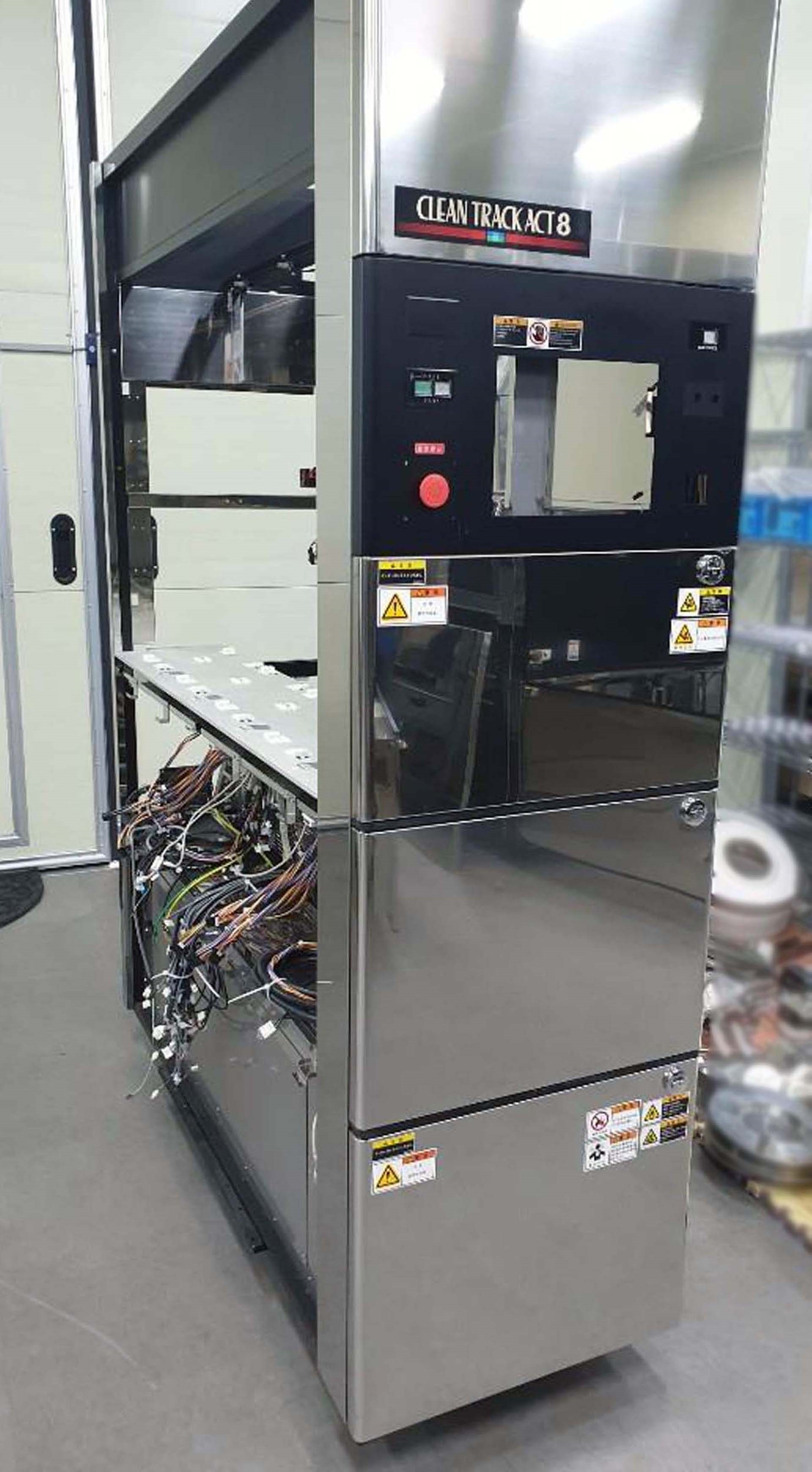
Used TEL / TOKYO ELECTRON ACT 8 #9252167 for sale
It looks like this item has already been sold. Check similar products below or contact us and our experienced team will find it for you.
Tap to zoom


Sold
ID: 9252167
Wafer Size: 8"
(2) Coater / (2) Developer system, 8"
I-Line
Single block system
Wafer flow: Left to right
Process block: Single block system
Block 1(C/S Blk):
CS Add on board missing
Main controller: ACT #2
Y,Z,Th Motor, X,Y,Z,Th Drive
Touch screen
Pincette
Block 2(P/S Blk)
(2) Spinner I/O boards missing
(2) Coater units (2-1, 2-2)
Direct drain type
(2) PR Nozzle assemblies
(4) Back rinses
(2) EBR Nozzles
(2) Out cup assemblies
(2) Nozzle changer motors
(2) Spin motors & drivers
(2) Developer units: (2-3, 2-4)
(4) Back rinses
(2) H Nozzle assemblies
(2) Out cup assemblies
(2) Spin motors & drivers
Oven unit:
(7) LHP/ Low temperature hot plates
(4) CPL/ Chill plates
TCP
(2) TRS / Transfer stations
(2) ADH/ Adhesion process stations
PRA / Process block robotics arm:
Missing part: Pincette
TH Drive
PRA Motor
Missing parts:
(4) ADH Inject valves
(10) Air valve (AMDZ1-X61)
(2) Spinner I/O boards missing (Coater units (2-1, 2-2) Developer units: (2-3, 2-4))
(2) DEV Drine bottles
Power cable
THC: T&H-NRE-2-A-00
Power box: PB2-U200-03-DV2
TCU.
TEL / TOKYO ELECTRON ACT 8 is a photoresist equipment that produces photomasks used in the production of semiconductor devices. This system has the capability to created highly accurate patterns with high resolution and repeatability. The photomask patterns it produces are created through the proprietary Double Patterning Exposure (DPE) method. This method involves exposing a single photoresist film to successive exposure from two different optical sources with scanning mirror projection. This unit also utilizes user-defined mask configuration with varying levels of image complexity and photomask geometry, enabling the user to customize the photomask patterns. The photomask produced by TEL ACT 8 is made through a variety of processes. First, a glass substrate is coated with an amorphous silicon resin, which serves as the photomask pattern. Next, the film is exposed to light, which sets down the photoresist rule layer. The light causes the exposed resin to polymerize and become insoluble to a certain chemical solution. This results in the creation of an etching line pattern. Lastly, this pattern is transferred onto the glass substrate. The resolution of this photomask machine is quite impressive, with a minimum line/space of 0.08 microns and a consistent pitch up to 0.2 microns across an array of 8 million pixels, making TOKYO ELECTRON ACT 8 ideal for the most stringent semiconductor device fabrication applications. Its repeatability of less than 0.001 microns ensures excellent product quality and yields. Additionally, the design of TOKYO ELECTRON ACT 8 enables a fast exposure time, generally ranging from several hours to one day. TEL ACT 8 tool also features a set of sophisticated error-check and auto-correction software tools. These tools enable out-of-tolerance conditions to be corrected manually before the etched film is reviewed, ensuring intricate patterns are produced accurately. Thus, TEL / TOKYO ELECTRON ACT 8 is a reliable photoresist asset that can produce highly advanced photomask patterns with exceptional repeatability and precision.
There are no reviews yet