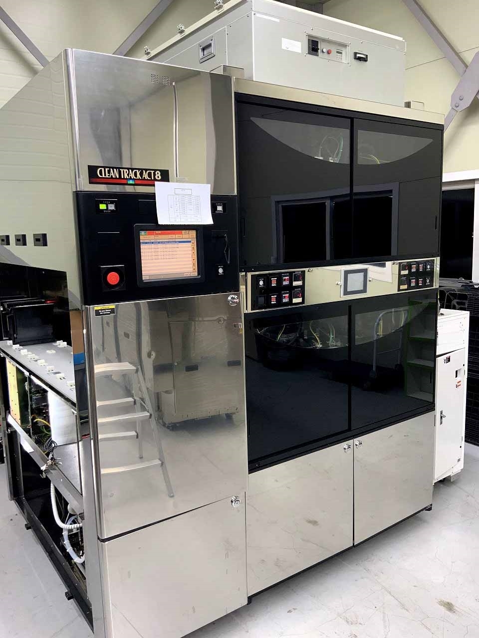
Used TEL / TOKYO ELECTRON ACT 8 #9283381 for sale
It looks like this item has already been sold. Check similar products below or contact us and our experienced team will find it for you.
Tap to zoom


Sold
ID: 9283381
Wafer Size: 8"
Vintage: 2003
(1) Coater / (2) Developer system, 8"
Machine type: L-Type
Single block
Main controller: M/C Normal installation
Coat Process Station (COT):
(2) Nozzles
RRC Pump
Solvent automatic supply: (2) Tank auto supplies / TEL Standard
Side rinse (EBR)
(2) Back Side Rinses (BSR)
Develop process station (DEV):
Nozzle
H Type
Dev Solution automatic supply: (2) Tank auto supplies / TEL Standard
Rinse nozzle
(2) Back Side Rinses
Adhesion process station
(6) Low temperature hot plate stations (LHP)
(2) High temperature hot plate process stations (HHP)
(4) Chilling plate process stations (CPL)
(2) Transition stage units (TRS)
AC Power box
Chemical box
Temperature controller
KOMATSU (SPA-1882-A) T&H
2003 vintage.
TEL / TOKYO ELECTRON ACT 8 is a photoresist equipment that is used to create high performance semiconductors. This system uses a data-driven optical lithography process, which is a form of direct write lithography. In photolithography, light is used to transfer patterned cells onto a substrate, typically a silicon wafer. This light is typically Ultraviolet radiation, or UV. This method of lithography allows the pattern to be precisely replicated and be scaled to fit the substrate. This becomes the starting point for creating transistors, capacitors, and other components of a semiconductor device. With TEL ACT 8, an advanced lithography machine is used that features a powerful 3-step process. First, the machine uses a binary optical mask to impose a specific pattern onto a blank silicon substrate. Next, this pattern is exposed to UV light, allowing the mask to then be removed. The finished product is an exact replication of the pattern on the mask. The unit alsofeatures an advanced wafer stage and a wafer scanning machine. These two components work together to ensure precision throughout the entire lithography process. The wafer scan tool is capable of moving the stages for positioning and alignment, in order to facilitate the most accurate patterning possible. This scan asset also helps reduce the processing time for each wafer. The 3rd step of the process is to coat the wafer in a photoresist material. This material is sensitive to UV light, so when it it exposed, only certain regions of the wafer will remain exposed. This process can be used to create patterns with greater detail than the previous binary optical mask, such as fine lines and small features. TOKYO ELECTRON ACT 8 provides users with a means of creating complex semiconductor designs quickly, accurately, and precisely. This model is perfect for a variety of industries and applications, including automotive, telecom, and consumer electronics. Its accuracy and efficiency allow for the production of highly-reliable and complex semiconductor parts.
There are no reviews yet