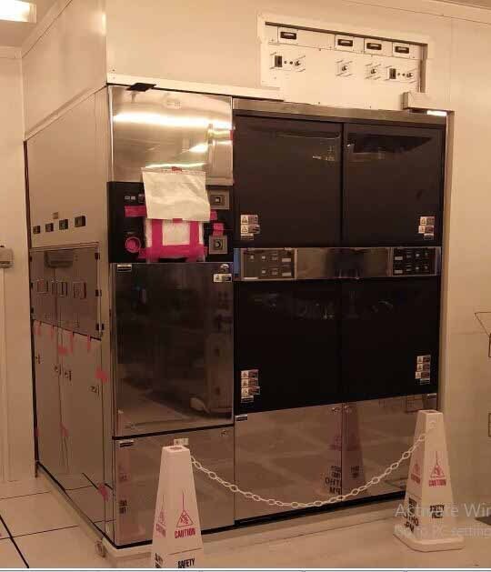
Used TEL / TOKYO ELECTRON Clean Track ACT 8 #9284114 for sale
It looks like this item has already been sold. Check similar products below or contact us and our experienced team will find it for you.
Tap to zoom


Sold
ID: 9284114
(2) Coater / (2) Developer system
Single block
Positive resist coater
(4) Load port stations IN/OUT
Type IV ACT Controller
(4) Uni Cassettes Stations (UNC)
(2) Chill Plate units (CPL)
(2) Adhesion units (ADH)
(9) Low Temperature Hot Plate units (LHP)
Transition unit (TRS)
Transition Chill Plate unit (TCP)
(3) INR-24-264A Circulating pumps
(3) INR-244-216C Circulating pump power supplies
(2) INR-244-217B CPL Power supply modules
INR-244-218F Controller
Coater unit:
(6) Resist nozzles
Unit / Nozzle / Pump / Tank type
2-1 COT / 1 / IWAKI HV-115-1, HV / LE Tank
2-1 COT / 2 / F-T100-3, RCC / LE Tank
2-1 COT / 3 / - / -
2-2 COT / 1 / IWAKI HV-115-1 HV / LE Tank
2-2 COT / 2 / F-T100-3 RCC / LE Tank
2-2 COT / 3 / - / -
Developer unit: Stream nozzle
2012 vintage.
TEL / TOKYO ELECTRON ACT 8 is a photoresist equipment designed for advanced photolithography applications. It is an advanced mask alignment and high-precision photolithography equipment that utilizes a combination of a mask aligner overlay and advanced photoresist technology. The system includes two cutting-edge technologies; the Mask Alignment Overlay (MAO) and the Photoresist Chemistry and Optimization (PCE). The Mask Alignment Overlay (MAO) is a key technology used in combination with electron beam (EB) mask alignment systems to accurately align layers of photoresist material onto a wafer substrate. The MAO aligns each layer with a quick and easy process, allowing for precise accuracy in even the most tightly toleranced components. The photoresist layer can be finely tuned through the MAO unit, optimizing the dosimetry of the photoresist material and reducing any possible overexposure during the lithography process. The Photoresist Chemistry and Optimization (PCE) machine provides precise control over the chemistry of a given lithography process, allowing for pre-programmed recipes and customized lithography parameters to be entered into the tool. This enables easy optimization of the photoresist layer and allows for tailored doses of a specific photoresist compound to be added prior to EB mask alignment. TEL ACT 8 offers a wide range of advantages to semiconductor manufacturers and researchers. It allows for the optimization of photoresist layers within a single-mask aligner wafer for reduced time of exposure and improved accuracy. The PCE asset enables easy and precise control of the photoresist chemistry for tailored doses of a specific photoresist compound. This produces superior repeatability and throughput, as well as reduced costs in manufacturing cycles. In order to take full advantage of TOKYO ELECTRON ACT 8, it is necessary to understand its benefits and capabilities. The model provides increased accuracy and precision in EB mask alignment, and its sophisticated MAO technology allows for optimized dosimetry of the photoresist material. Its optimized recipes and PCE equipment enable easy control of the photoresist chemistry, leading to improved reproducibility and throughput, and ultimately reducing long-term costs.
There are no reviews yet