Used TEL / TOKYO ELECTRON ACT 8 #9314468 for sale
URL successfully copied!
Tap to zoom
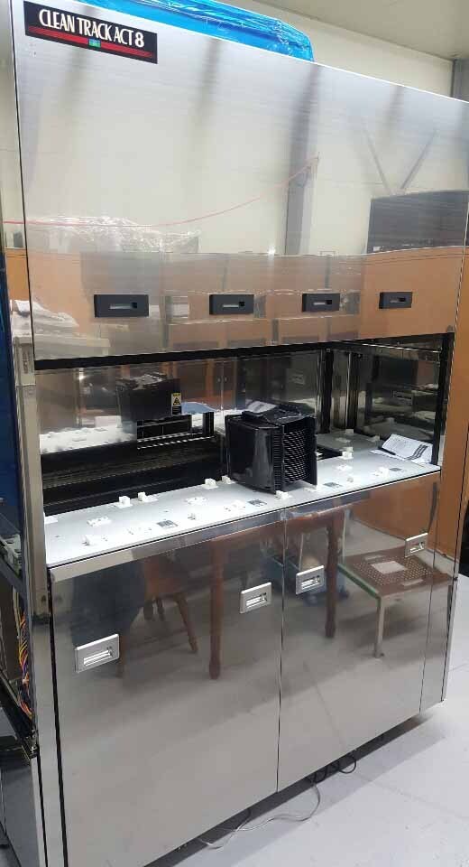

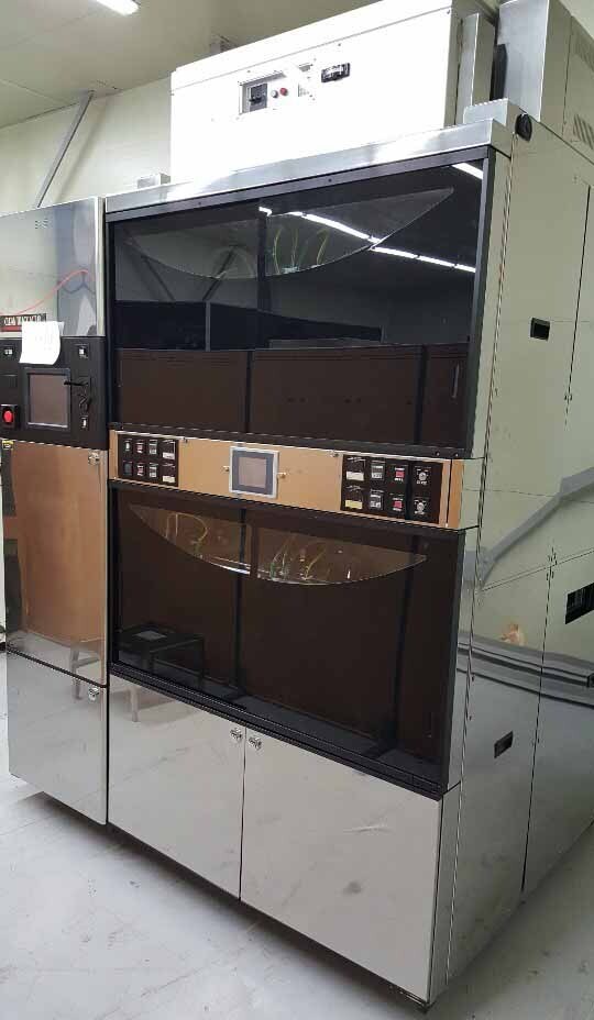

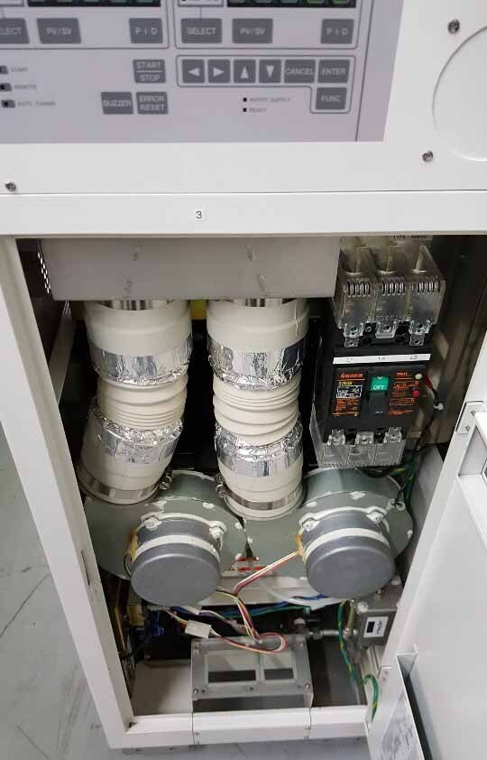

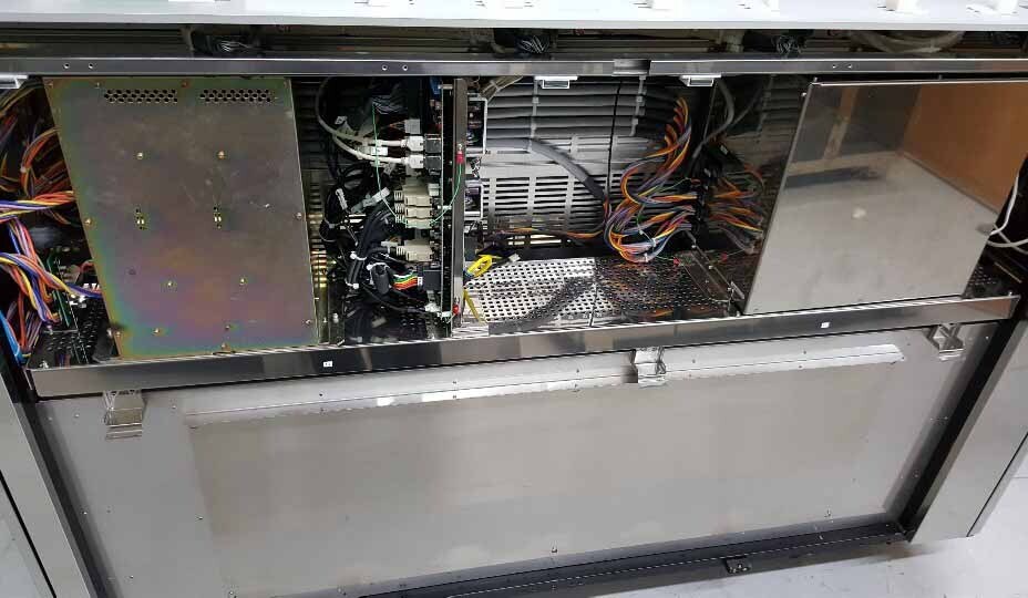

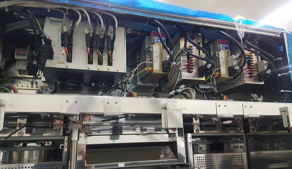

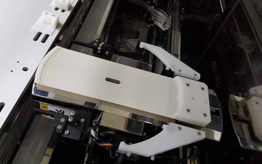

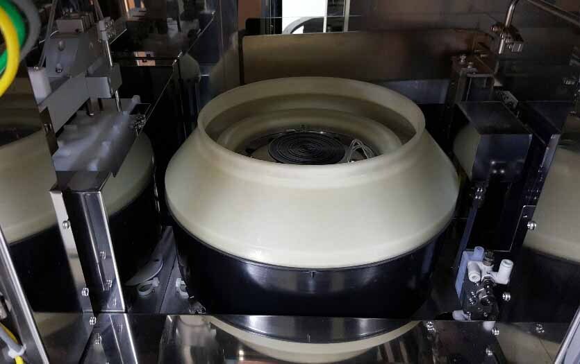


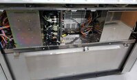
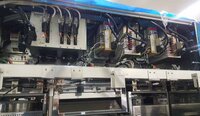
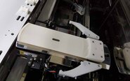
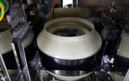
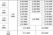
TEL / TOKYO ELECTRON ACT 8 is a photoresist equipment designed specifically for lithography applications. Its main purpose is to provide a precise control of the resist coating on the substrate, enabling the exposure of micron-scale features such as contact holes. The system consists of several components, each fulfiling a specific purpose. The main components are: A vacuum track: this is made out of stainless steel and allows the substrate to move through the various stations inside the unit. It also helps to ensure a uniform resist coating. A wafer placement machine: this utilizes a stepper motor to precisely locate the substrate to an exact position inside the tool. A coating chamber: this is where the resist is applied and baked onto the substrate. The chamber also controls the environmental conditions inside the chamber to achieve a uniform resist coating. A resist applicator: this applies the resist to the substrate using a spin coating process. A high resolution thermal imaging asset: this model allows the exposure of micron-scale features such as contact holes. It consists of a heating element and a cooling lines that move around the substrate and precisely control the temperature. A laser beam exposure equipment: this system uses a laser beam to expose the pattern on the photoresist layer on the substrate. Overall, TEL ACT 8 photoresist unit is designed to provide a reliable and precise control of resist coating on the substrate, ensuring satisfactory results. With a compact footprint and good thermal control, the machine can be used in a variety of applications. With its high-resolution imaging capability, it can also expose micron-scale features with ease. The tool also provides users with a variety of settings to optimize the process for each user's specific requirements. This makes it a valuable tool for lithography applications, and essential for advanced microfabrication processes.
There are no reviews yet


