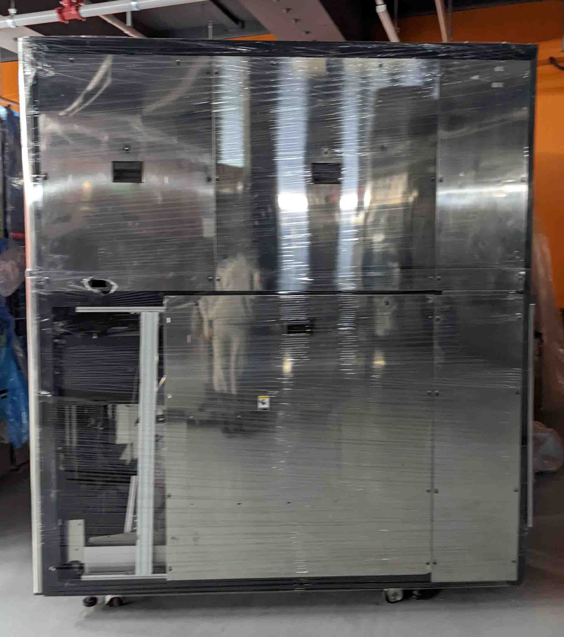
Used TEL / TOKYO ELECTRON Clean Track ACT 12 #293592464 for sale
It looks like this item has already been sold. Check similar products below or contact us and our experienced team will find it for you.
Tap to zoom


Sold
TEL (TE) TEL / TOKYO ELECTRON Clean Track ACT 12 is a 'photoresist' equipment, used in the microelectronics industry for device fabrication. Photoresists are chemical formulations that are sensitive to specific energies of light. When exposed to light, the molecules within the photoresist react, resulting in a change in their molecular state. Typically, photoresists are deposited on wafers to create specific patterns, and these patterns can be used to build large-scale integrated circuits. TEL Clean Track ACT 12 system offers several advantages over traditional photoresist systems, including increased cleaning power, improved productivity, and cleaner results. Its ability to clean post-exposure deposits at the end of a process is especially beneficial. It is also fast and cost-effective, able to deliver excellent results in less than a tenth of the time needed by conventional systems. TOKYO ELECTRON Clean Track ACT 12 is equipped with a Spin/Spray Unit, which is used to apply the photoresist to the semiconductor wafer under a vacuum. The photoresist is placed in a spin/spray cup, which is a hollow plastic cup filled with the photoresist. The cup is then placed on a rotating spindle and spinned at an appropriate speed to evenly distribute the photoresist on the wafer. This process also ensures that the photoresist is evenly distributed over the entire surface of the wafer for consistent patterning results. Once the photoresist is applied to the wafer, it is exposed to the light source in Clean Track ACT 12 for the desired length of time. The machine has a high intensity mercury-vapor lamp that collimates the light for the best possible exposure uniformity. The photoresist is then developed in the tool's agitated bath of developer solution. This removes unexposed portions of the photoresist, leaving behind a pattern on the wafer. Finally, the asset is equipped with an advanced cleaning module, comprised of a cascade of spray heads that disperse several different solvents to accurately clean the residuum from the wafer. This automated cleaning technology provides superior cleaning results, and significantly reduces the amount of time and labor needed to achieve clean-tape brightness on the wafer. In summary, the TE TEL / TOKYO ELECTRON Clean Track ACT 12 photoresist model is an ideal solution for device fabrication. It provides superior cleaning performance, improved productivity, and a clean wafer that is ready for the next step in device fabrication. Its fast and cost-effective operation, combined with its automated features, make it an attractive choice for semiconductor manufacturers.
There are no reviews yet