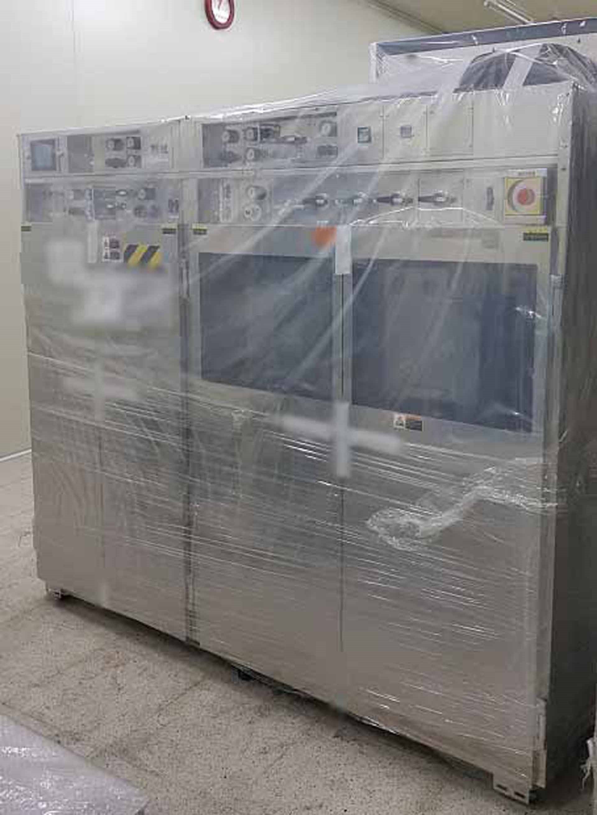
Used TEL / TOKYO ELECTRON Clean Track ACT 12 #9227624 for sale
It looks like this item has already been sold. Check similar products below or contact us and our experienced team will find it for you.
Tap to zoom


Sold
ID: 9227624
Wafer Size: 12"
Vintage: 2003
(1) Coater / (2) Developer system, 12"
Left to right
(3) Main controllers
In-line
CSB
IFB
PRB 1
Power box
Chemical box 1
Fire system box 1 and 2
T&H Controller 1
Thermo controller 1
Loading configuration:
(3) FOUP Loaders
Uni-cassette
With system controller
Carrier station:
Type: FOUP
(3) Cassettes
Uni-cassette system
Coaler unit:
(6) Dispense nozzles
With temperature controlled lines for etch unit
RDS Pump (Millipore)
Rinse nozzle: Back / EBR / Solvent bath for etch unit
Rinse system:
(3) Liters
(2) Tanks
Buffer tank system
Degassing system
Programmable side rinse
PR Nozzle (1, 2, 3, 4, 5,6)
(6) Bottles (1 Bottle / 1 Nozzle)
Thinner supply: CCSS
AMC Suck-back valve
Drain: Direct drain
Developer unit:
H Nozzle
Stream nozzle for DI rinse
(2) Points for back side rinse
Developer system:
(3) Liters
(2) Tanks
Buffer tank system
Developer supply: CCSS
Degassing system
Developer temperature control system
Drain: Direct drain
I/F Wafer stage type: NIKON SF130
Adhesion unit
Chamber (Build-in hot plate)
HMDS Tank with float sensor
HMDS Supply: Local bottle
(5) Low temperature hot plates (LHP)
(4) Chill plates (CPL)
(2) Precision chilling hot plates (PHP)
TCP Unit
(2) TRS Units
Wafer edge exposure (WEE)
UV Sensor: I-Line
Chemical cabinet:
Solvent
HMDS
DEV Chemical cabinet
SHINWA Series (ESA-8) Temperature and humidity controller
Temperature control unit (TCU)
AC Power box
2003 vintage.
TEL / TOKYO ELECTRON Clean Track ACT 12 is a photoresist equipment that is used for photolithography by creating a thin film pattern on the surface of a wafer. The system uses a dedicated clean track that prevents the contamination of the wafer surface during the exposure process and offers improved process capability as compared to other conventional systems. The unit is designed to achieve higher resolution patterns and better repeatability. It has a vacuum machine as well as a baking process that actively works to dry the photoresist and produce better pattern accuracy. The tool is equipped with a dedicated cleansing track for wafer pre-cleaning and a main track for exposing. The pre-cleaning track incorporates an oxidation process which helps to purify the wafer surface and improves the film quality for photomachining. The pre-cleaning also eliminates any contamination caused by airborne dust particles or other surface contaminants. The main track is designed to offer a stable low voltage power supply, which ensures high power stability for the exposure process. A high-precision optics asset is incorporated in the main track, which ensures accuracy and stability in the exposure process. The model has various programmed operation cycles which can be customized according to the requirements of the user. It also has built in safety features which helps to prevent any accidents and damage to the equipment. It has a large user friendly display screen which allows the user to access all the functions of the equipment easily. The system also has an algorithm driven optimization unit which allows the user to optimize the exposure time and process conditions to achieve desired pattern accuracy and process yield. It also ensures uniformity of the thin films created upon exposure and offers better process capability. The machine can also be interfaced with other systems such asetching, deposition, and stripping equipment, to offer improved processing speed and better pattern quality. Overall, TEL Clean Track ACT 12 is a powerful photoresist tool capable of achieving high levels of accuracy and repeatability. It has a host of features tailored towards achieving precise pattern results and ensures superior yield of the finished wafer. The asset is designed to offer reliable and efficient performance, which enables users to produce high quality products and reduce waste.
There are no reviews yet