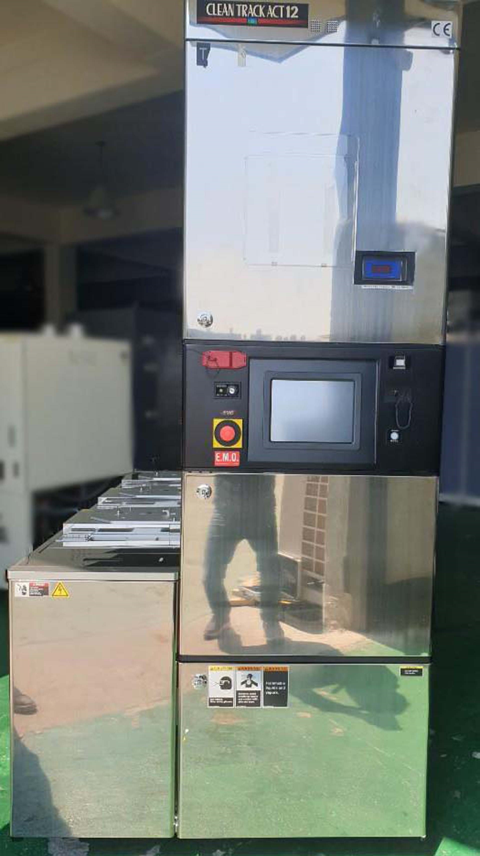
Used TEL / TOKYO ELECTRON Clean Track ACT 12 #9242356 for sale
It looks like this item has already been sold. Check similar products below or contact us and our experienced team will find it for you.
Tap to zoom


Sold
ID: 9242356
Wafer Size: 8"
(2) Coater / (4) Developer system, 8"
Dual block system
Wafer flow: Left to right
Block 1:
C/S Block, 12"
Stage / Indexer:
Non-SMIF / Open uni-cassette
CSB / Cassette stage block
Block 2:
P/S Block, 12"
(2) Coat units: 2-1 & 2-2
E-Box
Cup base, 12"
(2) PANASONIC Motor drives
PRA / Process block robotics arm
Pincette, 12"
(4) HCP
(4) LHP
TCP
(2) ADH / Adhesion
SHU
Block 3:
P/S Block, 12"
(4) Developer units: 3-1, 3-2, 3-3 & 3-4
E-Box
Cup base, 12"
Out cup, 12"
(4) YASKAWA Motor drives
(4) H Nozzles 1 & 2
PRA / Process block robotics arm
Pincette, 12"
(4) PHP
(4) LHP
(3) HCP
Block 4:
I/F Block, 12"
WEE Unit
CPL
IF Arm
Chemical supply cabinets: (2) Coater & (4) Developer
Power transformer AC cabinet
Temperature & humidity controller: SHINWA T&H ESA-8
TCU: (2) ACT 12 Frames
Missing parts:
Block 2 (P/S Block):
(2) Spin I/O boards
(2) Spin motors
(2) Out cups
(2) PR Nozzle assy
Air sol V/V
Oven:
(2) E5ZE
Z Motor
Lower drain sheet metal & hardware
Block 3 (P/S Block):
Developer:
(4) Spin I/O boards
(4) Spin motors
Oven:
PHP Flow meter assy box
E5ZE
REX Controller.
TEL / TOKYO ELECTRON Clean Track ACT 12 is a high-quality photoresist equipment that combines reliable lithography with automated process systems. The system is designed to facilitate high-volume lithography in the production of silicon chips. The unit contains an ion beam machine, submersible cooling tool, exposure chamber, and an in situ optical asset. The ion beam model is responsible for the precise etching of the photoresist. The submersible cooling equipment helps to reduce thermal stress and contamination levels in the system. The exposure chamber emits an active radiation to the photoresist material to be developed. This radiation can be selected from a variety of wavelengths. The in situ optical unit is responsible for controlling light intensity. This feature is important, as it allows the photoresist machine to accurately reproduce chip designs. The activation of TEL Clean Track ACT 12's features is done in stages. First, the required optical settings are inputted and then the photoresist is exposed to the radiation. After the exposure process is complete, the ion beam tool is actuated; this helps to etch the photoresist material. Finally, the submersible cooling asset is enabled to reduce thermal stress and contamination levels. TOKYO ELECTRON Clean Track ACT 12 is also equipped with an alarm and/or monitoring model. This helps to detect any faults in the process, and it can also provide maintenance data. This feature ensures that the photoresist equipment runs efficiently and prevents any potential damage to the system. Clean Track ACT 12 is a highly efficient and reliable unit for lithography. It is capable of producing high-precision pattern designs and can easily be combined with automated process systems. This feature is especially beneficial in the production of silicon chips. The combination of the ion beam machine, submersible cooling tool, exposure chamber, and in situ optical asset ensures that the photoresist is accurately etched and exposed to the desired wavelengths. The alarm and monitoring model further enhances the equipment's efficiency and reliability.
There are no reviews yet