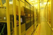
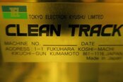
Used TEL / TOKYO ELECTRON Clean Track ACT 12 #9252495 for sale
URL successfully copied!
Tap to zoom
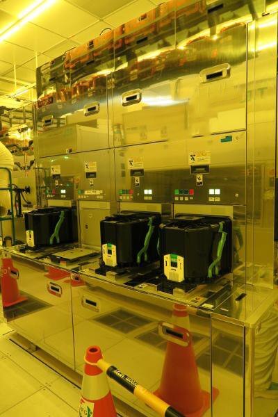


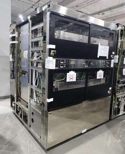

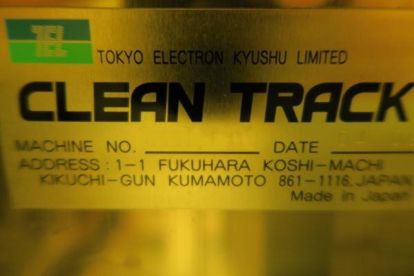

ID: 9252495
Wafer Size: 12"
Vintage: 2004
Coater / (2) Developer system, 12"
FOUP
Modules:
(4) COT
(9) LHP
(6) HHP
(4) PHP
2004 vintage.
The 'TEL / TOKYO ELECTRON Clean Track ACT 12' is a photoresist equipment used for the development of semiconductor-based devices. The system allows for the precise patterning of circuits, such as integrated circuits, through the use of advanced exposure and post-exposure processes. TEL Clean Track ACT 12 is an automated unit which operates under the Photolithography Exposure Method. This method involves the use of a clean room and a variety of tools and technologies to accurately etch intricate patterns onto a silicon wafer. Competitive technologies such as optical proximity correction (OPC) and process control are utilized to ensure precision process control. TOKYO ELECTRON Clean Track ACT 12 allows for the use of high-resolution panels and laser direct imaging (LDI) to make tiny structures. This machine is equipped with a hot plate, a spin-coater, a liquid dispenser, and a TEL Zeus exposure module. Each of these components, when combined with the photolithography technology, allows for the most precise and accurate patterning of circuits. The spin-coater is used to uniformly disperse photoresist onto the wafers, while the hot plate is utilized to heat the photoresist. The liquid dispenser, which is vacuum assisted, helps to dispense uniform amounts of photoresist to ensure consistency. TOKYO ELECTRON Zeus module enables a laser direct imaging process which allows for exposure of 12 wafers at a time. The vacuum-assisted liquid dispenser is a key component of Clean Track ACT 12. This feature helps to achieve high levels of uniformity, accuracy and profile control of the photoresist. This combination of elements ensures that the photoresist is free from debris, thus providing cleaner walls and better performance and yield in the production of semiconductor-based components. Finally, TEL / TOKYO ELECTRON Clean Track ACT 12 provides users with the ability to control the process. It has a built-in process control software tool that allows users to monitor the process and calibrate settings to produce precise patterns. This helps to reduce defect rates and optimize process control for more efficient photolithography development. In conclusion, TEL Clean Track ACT 12 is a highly advanced photoresist asset used for the development of semiconductor-based devices. It uses a variety of tools in combination with advanced exposure and post-exposure processes to relieve the most accurate and precise patterning of circuits.
There are no reviews yet


