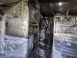
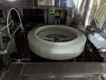
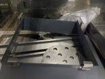
Used TEL / TOKYO ELECTRON Clean Track ACT 12 #9269255 for sale
URL successfully copied!
Tap to zoom


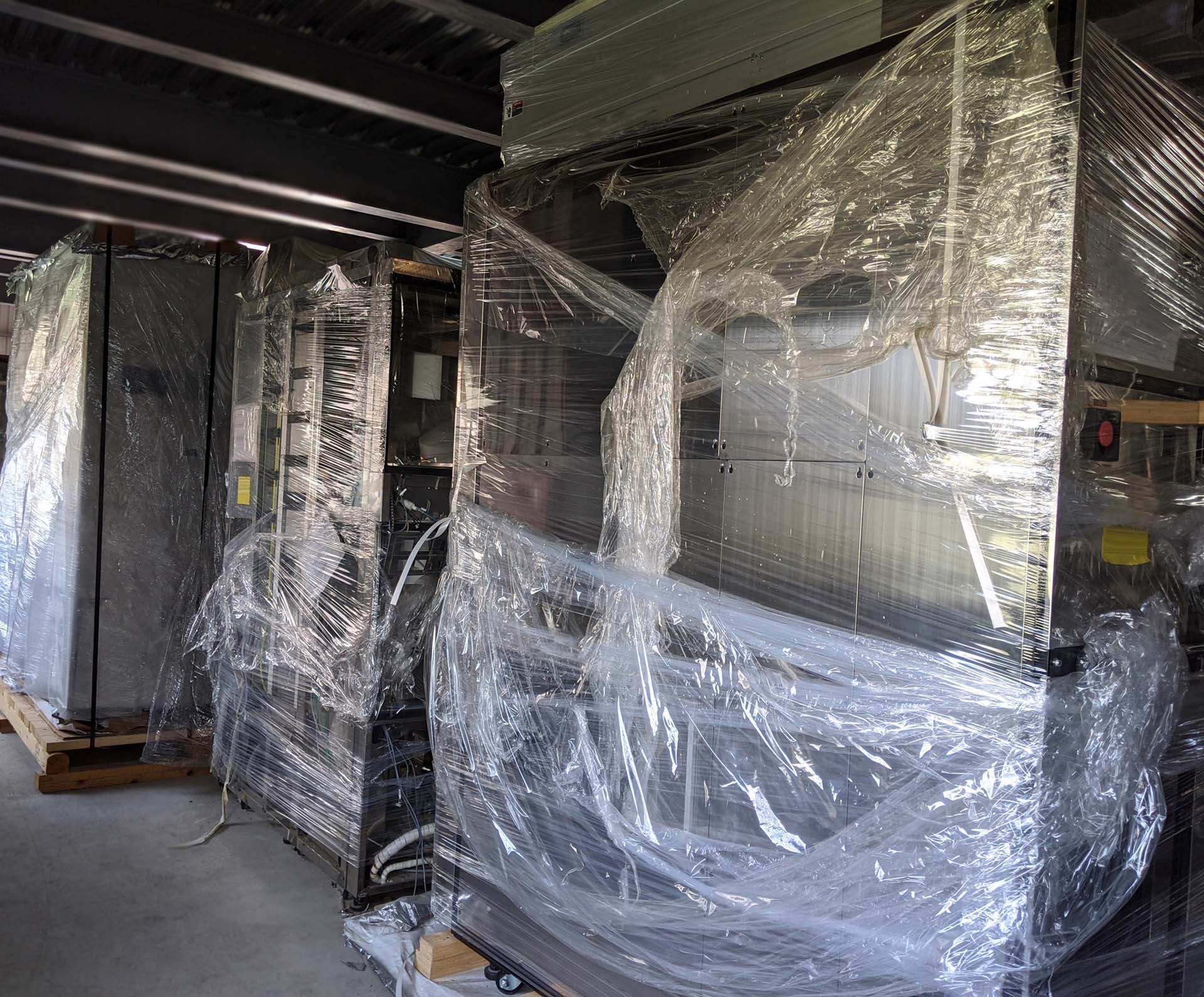


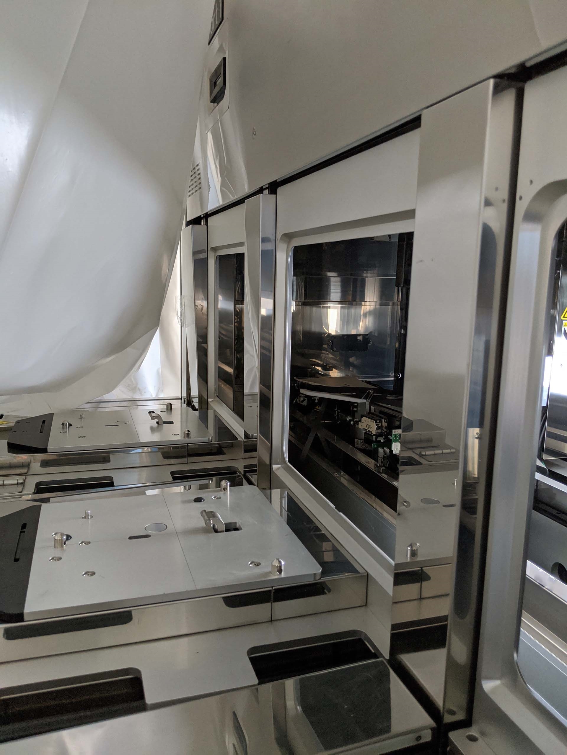

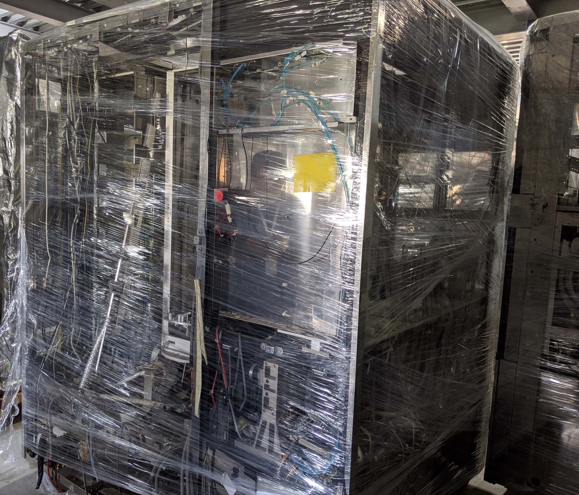


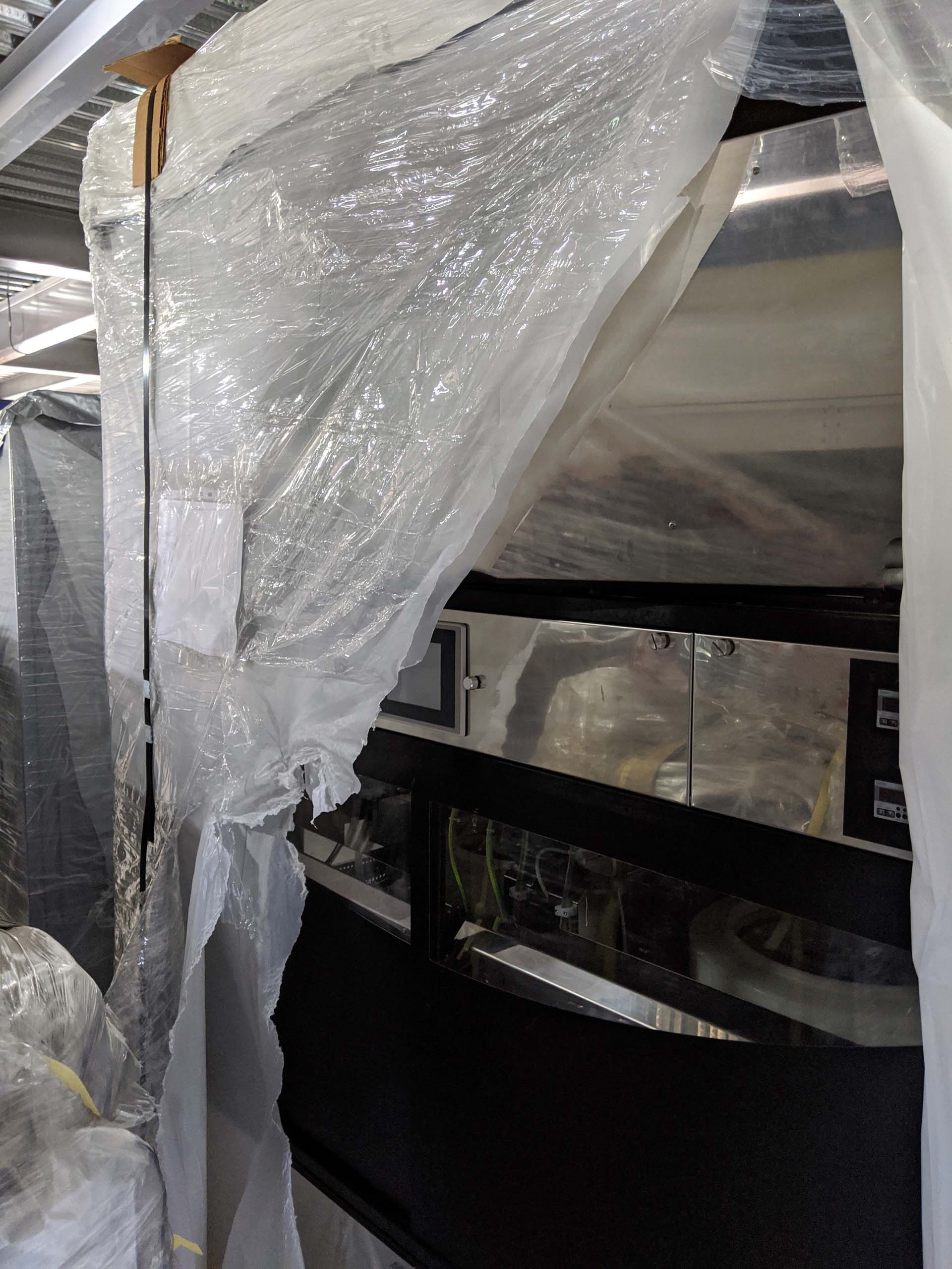


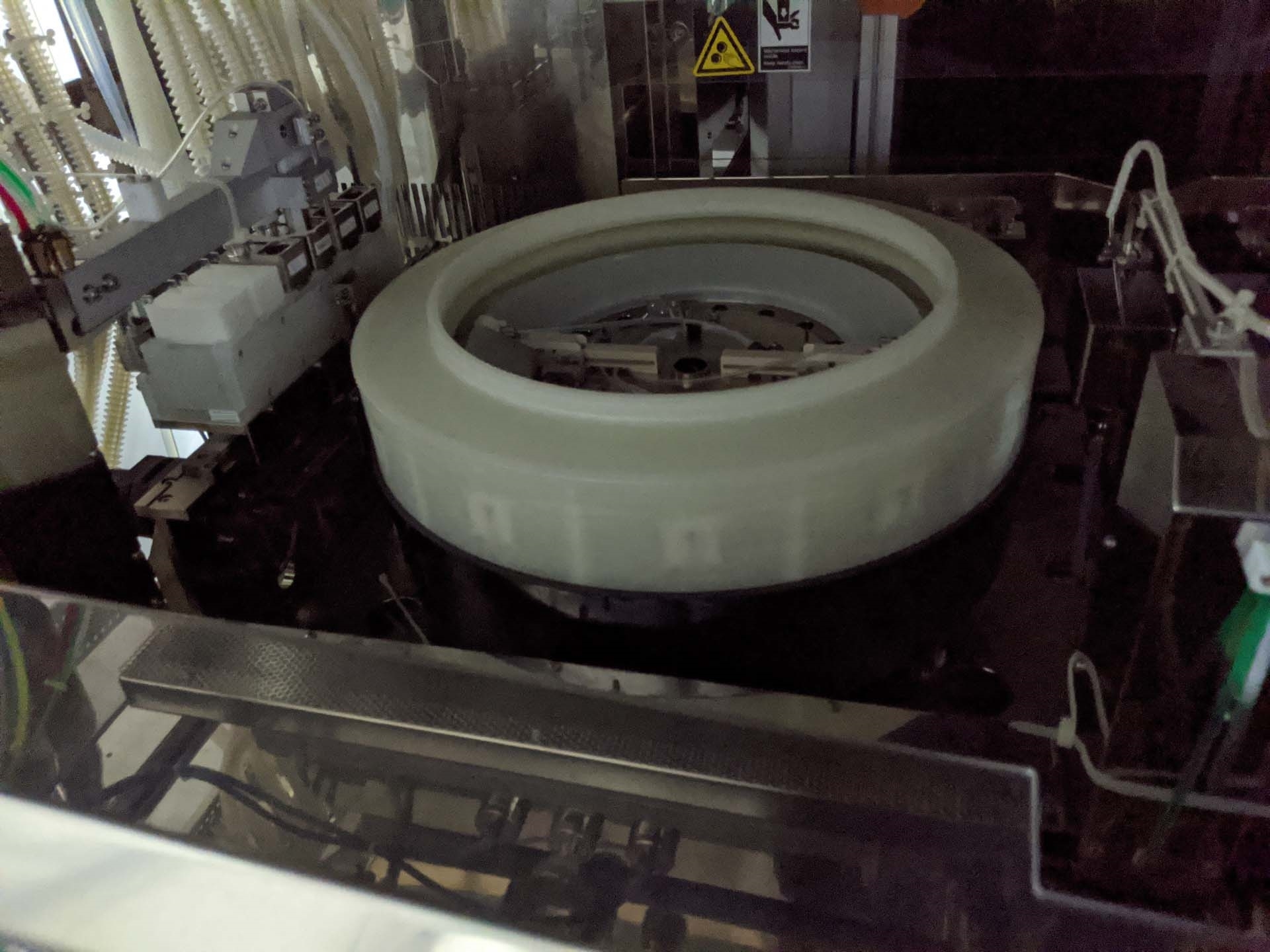

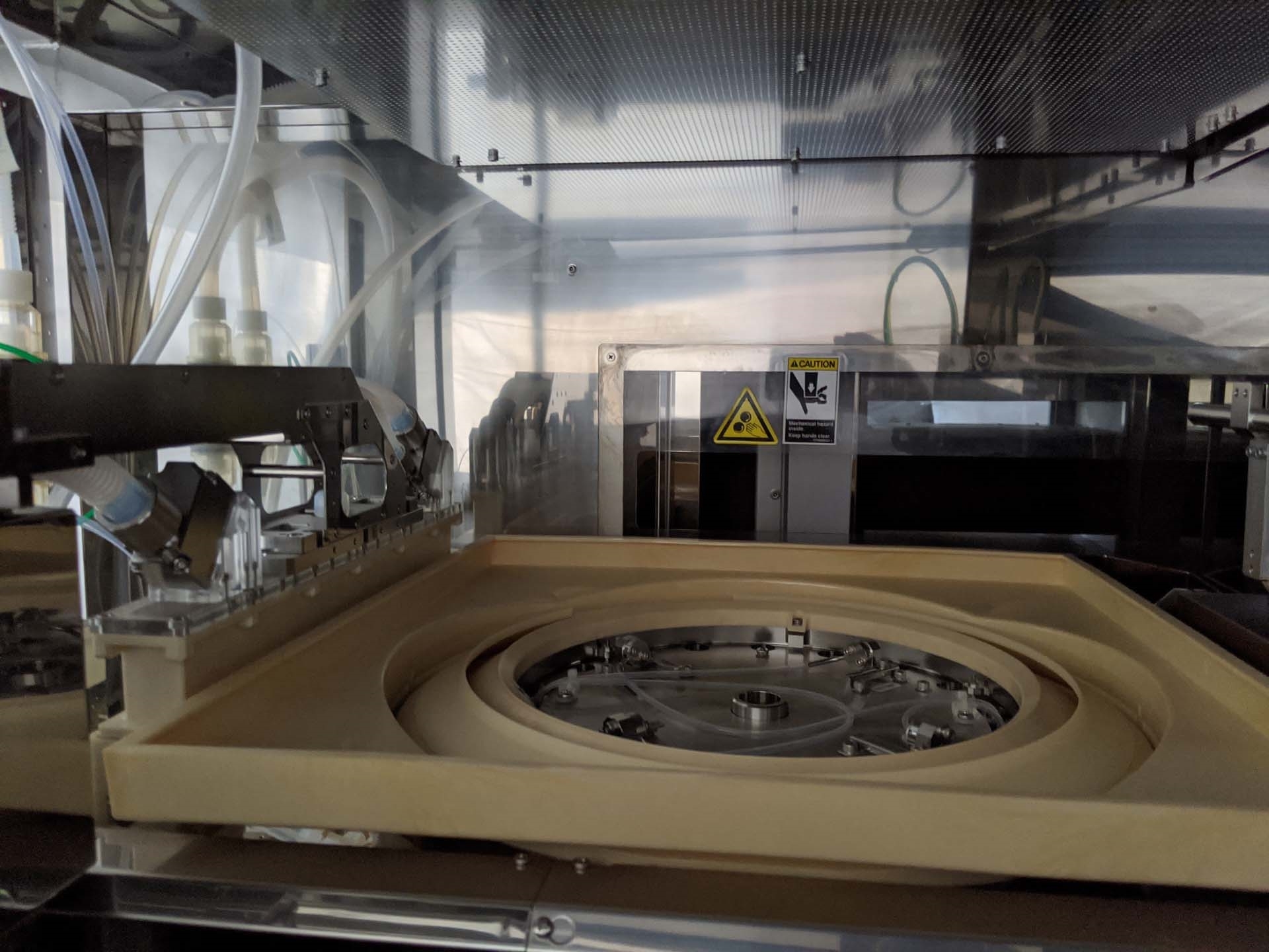

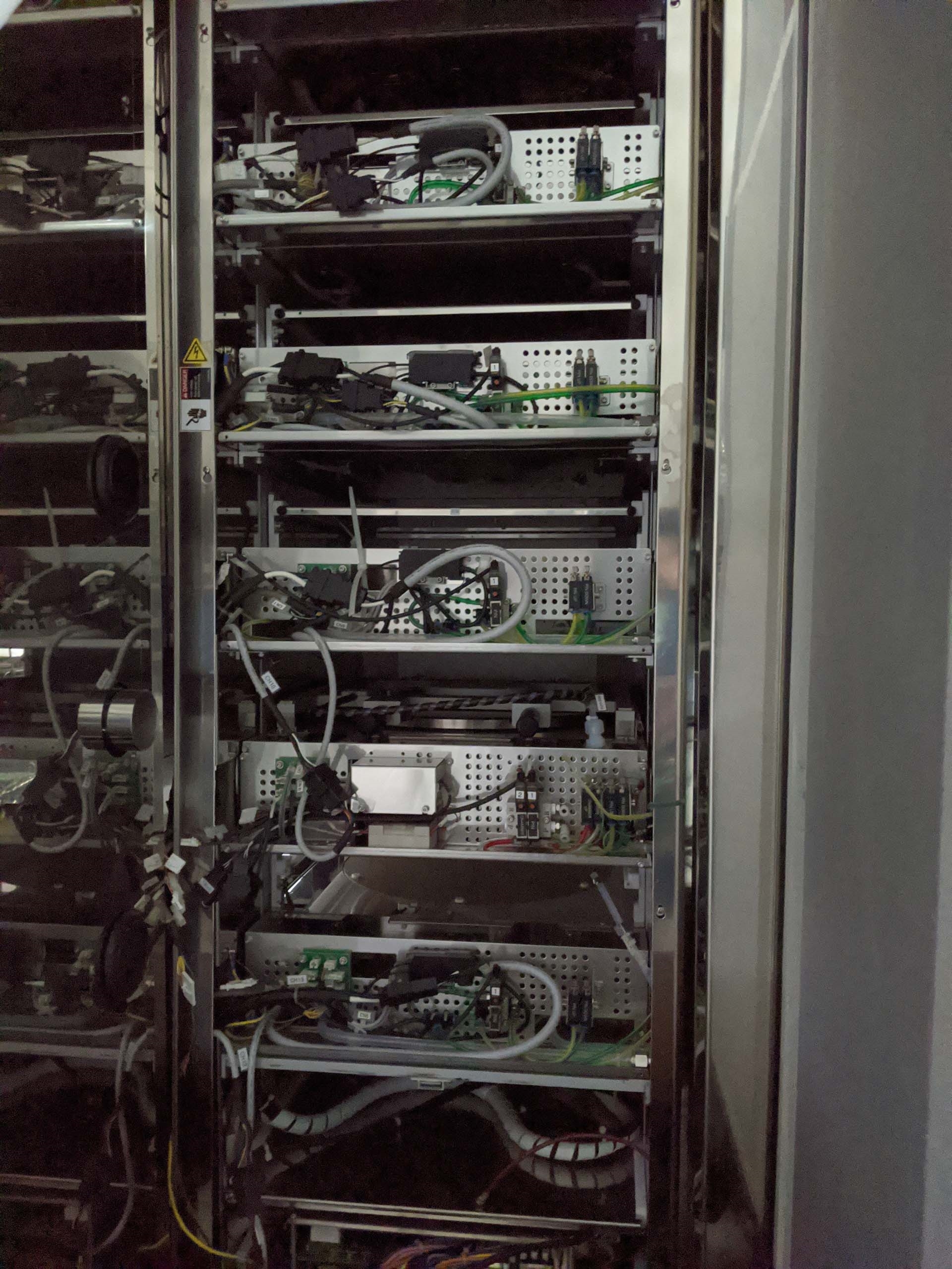



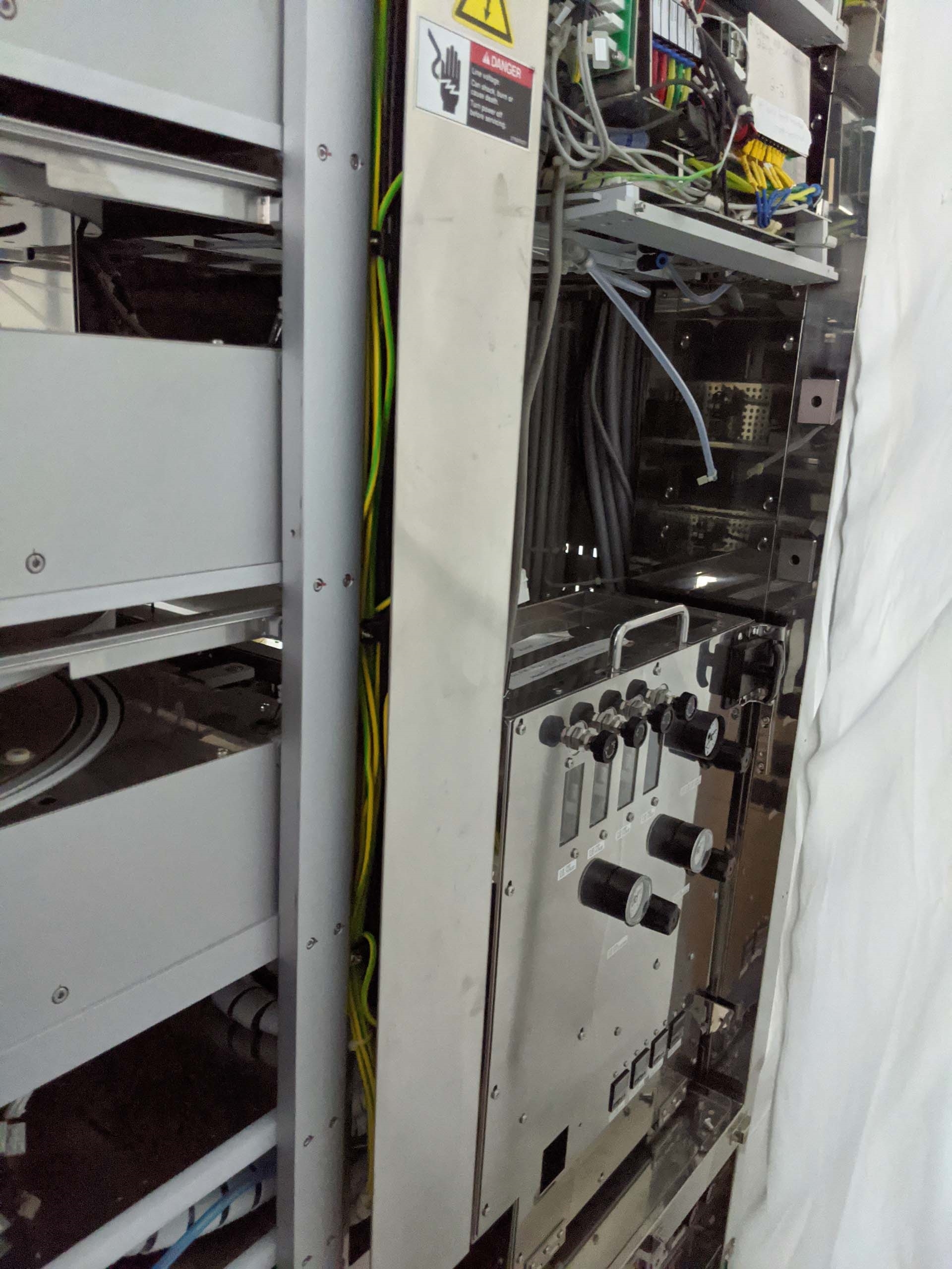

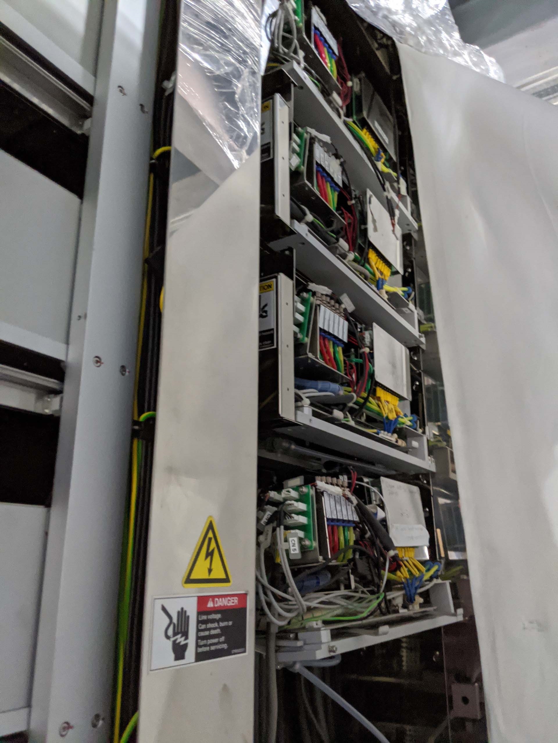

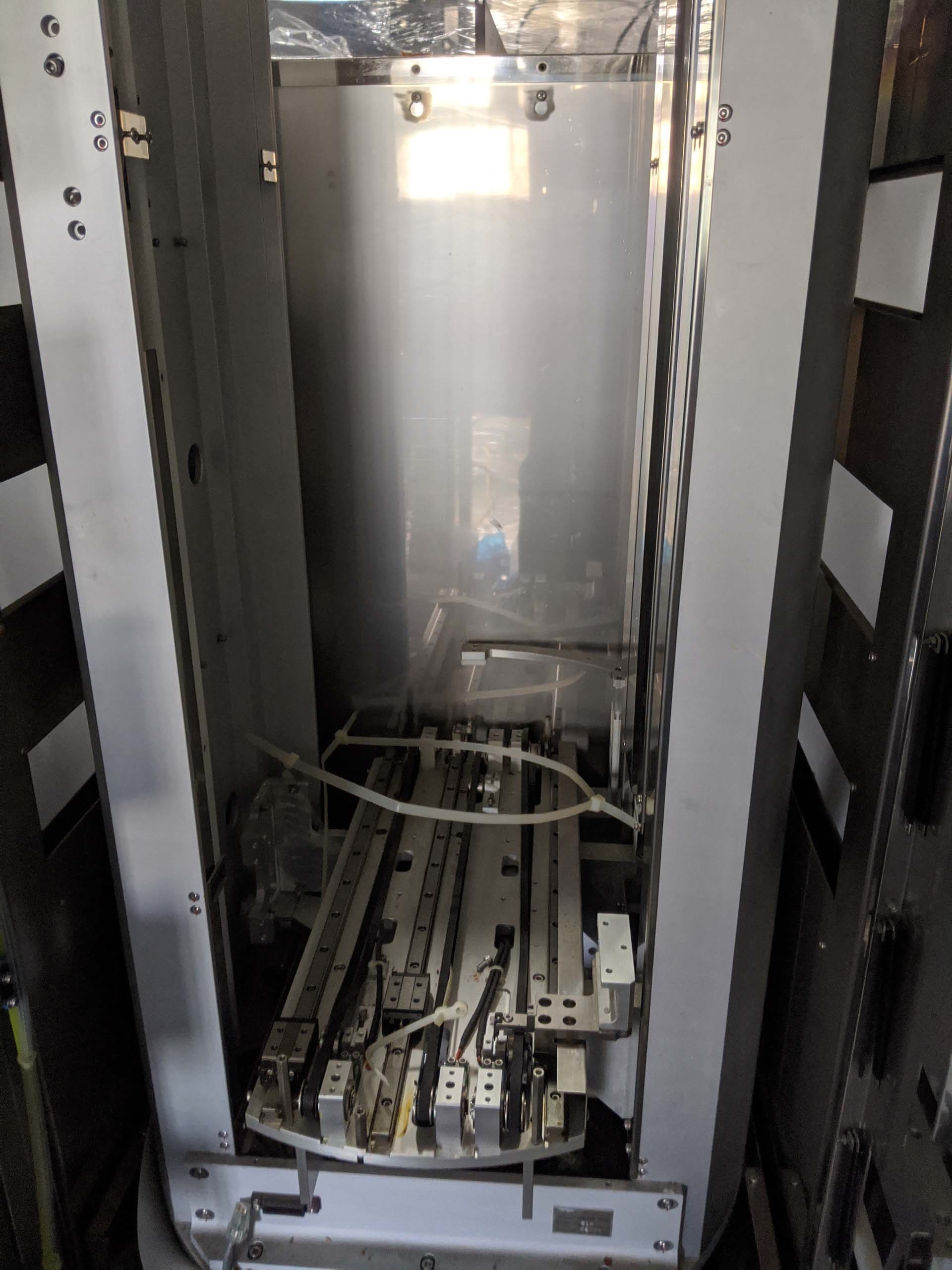


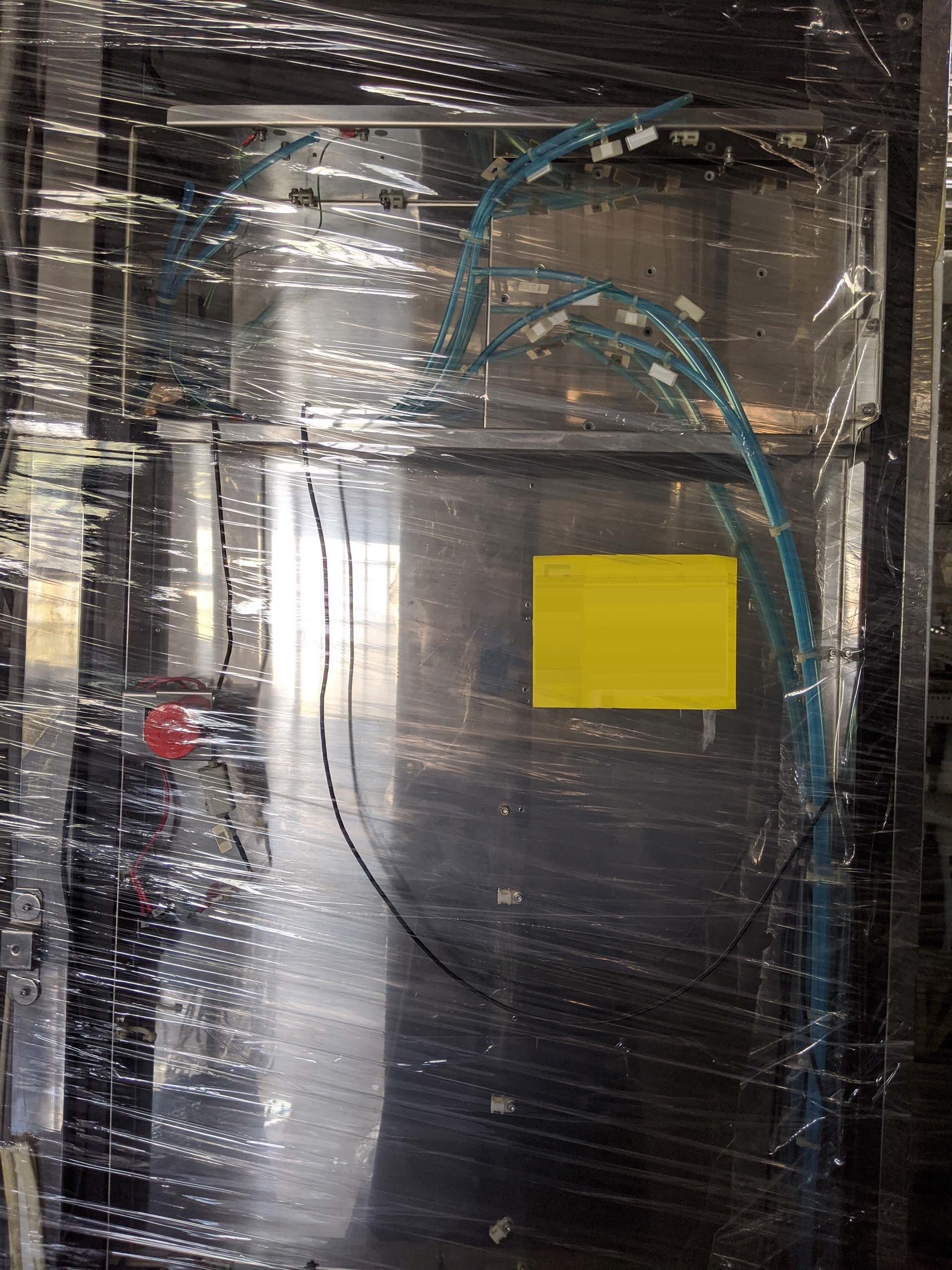

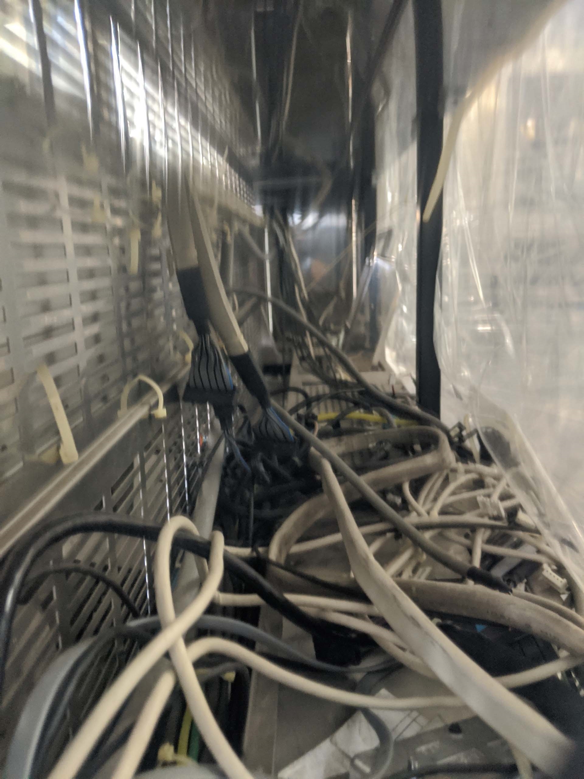

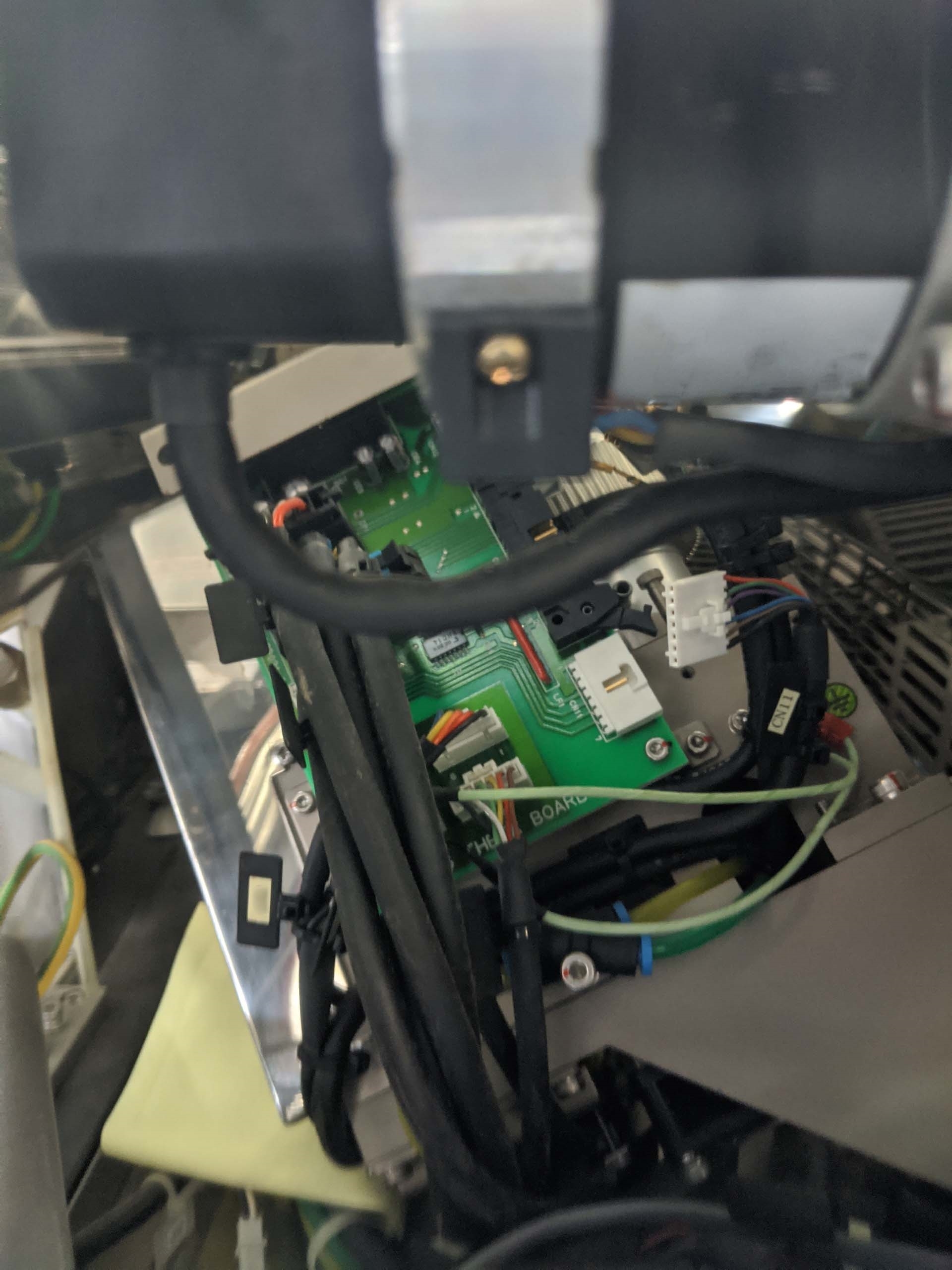

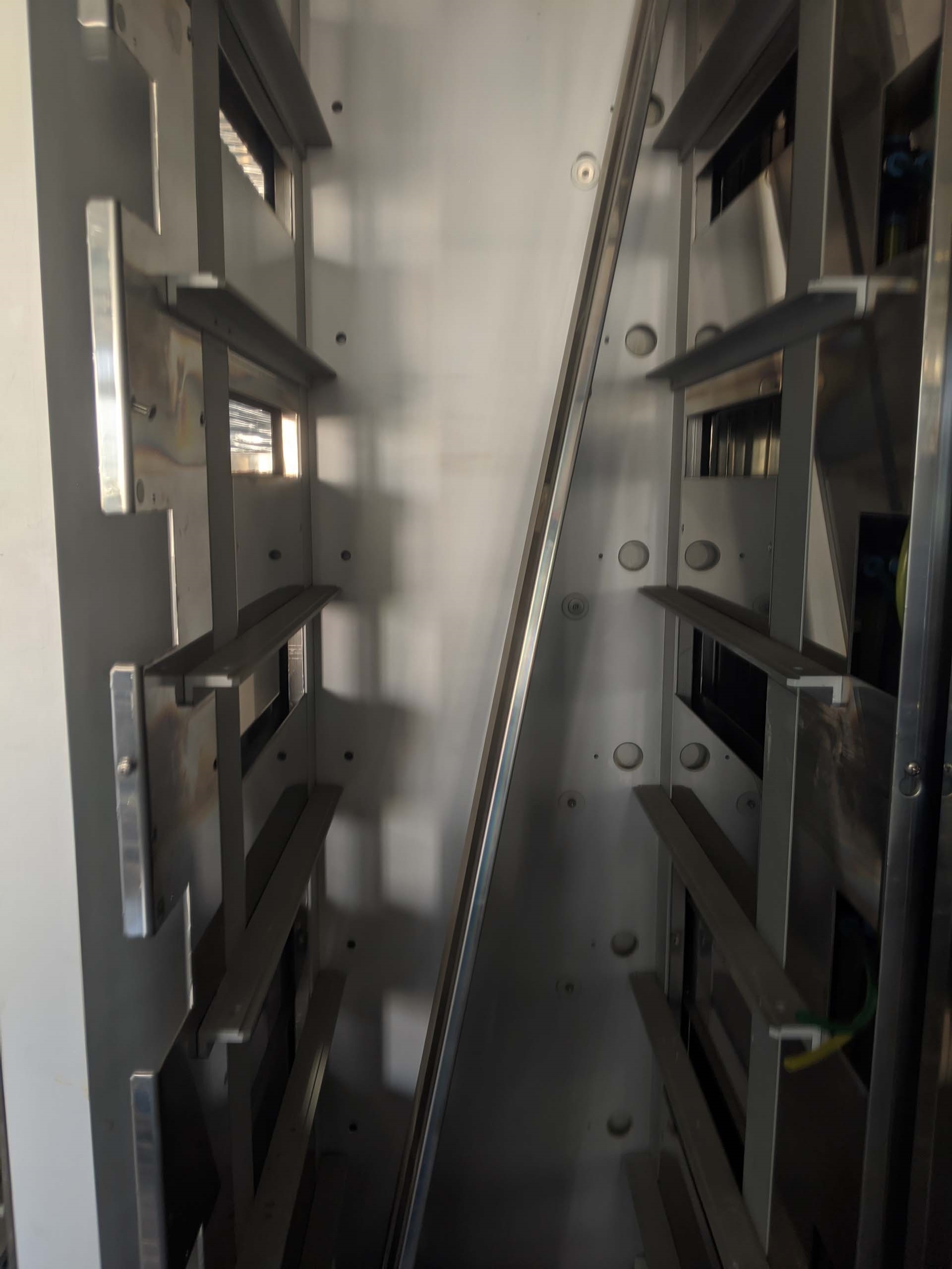

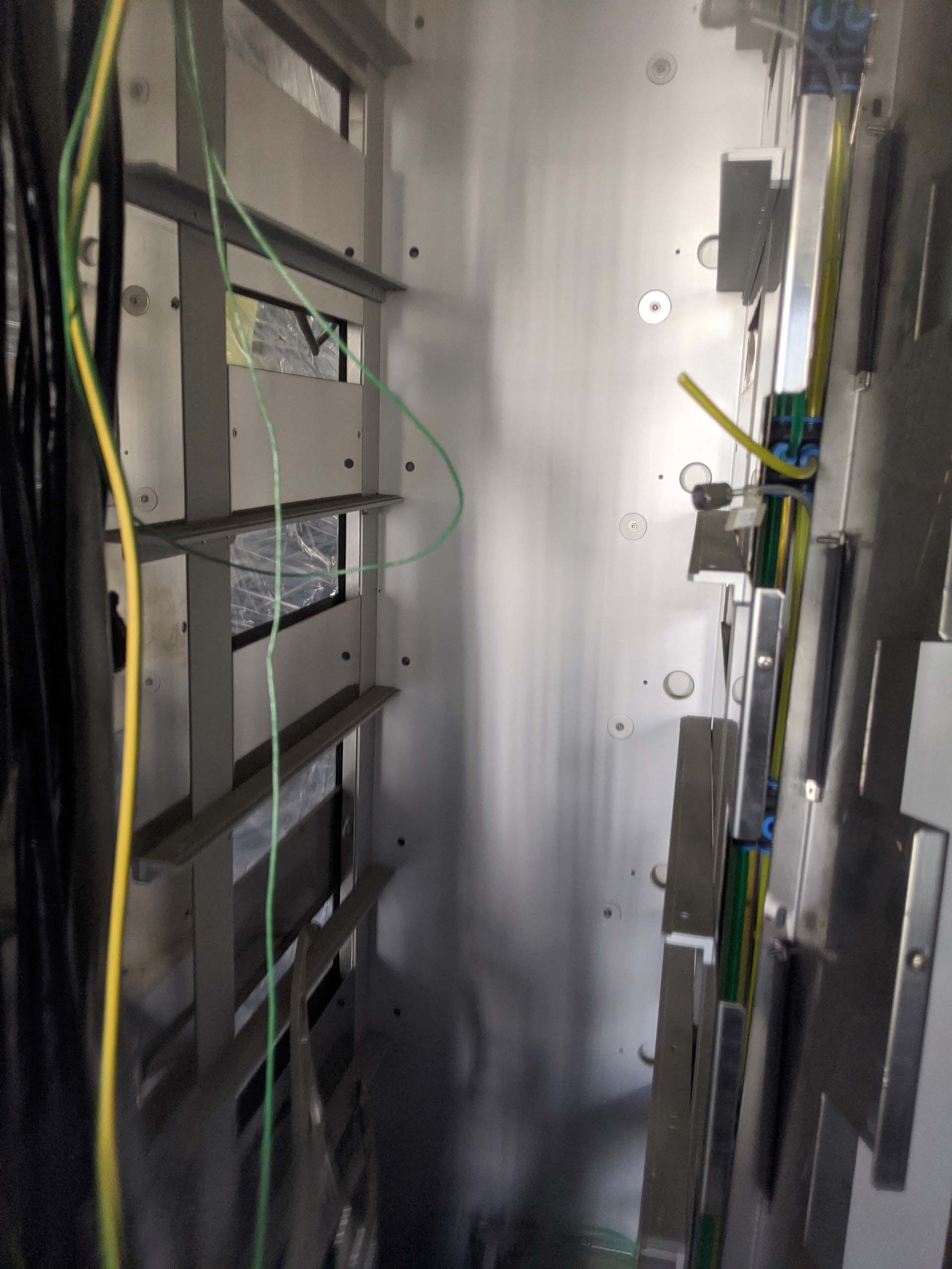

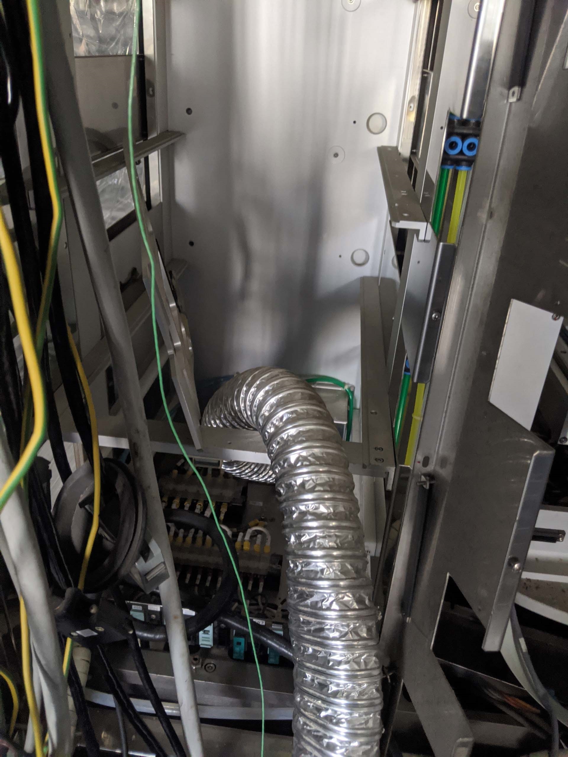


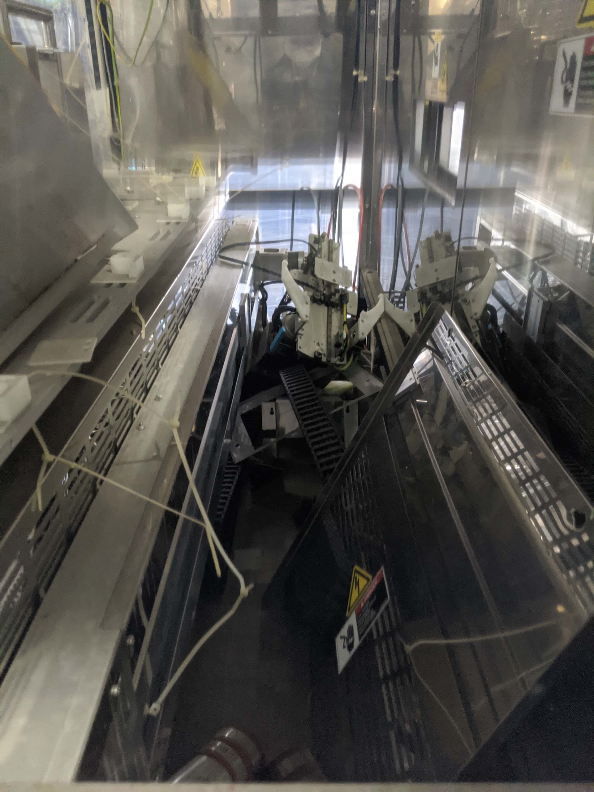


TEL / TOKYO ELECTRON Clean Track ACT 12 is a photoresist system designed for superior lithographic accuracy and process performance. Photoresist is a chemical process used in the production of integrated circuit components and other microelectronic devices. TEL Clean Track ACT 12 is two-step chemical materials based system, consisting of three major components: a positive photoresist resist, a pre-spin resist, and a negative photoresist. Positive photoresist resists are used in semiconductor fabrication processes such as contact etching, gate contact etching, dielectric etching, and polysilicon doping. This resist has a high sensitivity to ultraviolet (UV) light and produces a motion track pattern on the wafer surface. Pre-spin resist also plays an important role in semiconductor fabrication. It stabilizes the film structure and initiates the etching of the mask pattern. Finally, negative photoresist is used to remove the undesired portions of the pattern, without attacking the desired portions. TOKYO ELECTRON Clean Track ACT 12 provides superior lithographic accuracy due to its ability to precisely control the resist thickness, pattern CD and uniformity of the resist. This is achieved through its advanced film development monitoring, high-accuracy backside reflection tool, and other integrated process control functions. In addition, the system is equipped with an automated feed-through assembly, which is critical in producing components with consistent geometries and dimensions. Furthermore, Clean Track ACT 12 features a high-resolution elevator mechanism that permits a uniform resist gap between the wafer and the substrate. The result is high-quality wafer parts with reduced contamination, enhanced yield, and improved performance.
There are no reviews yet

