Used TEL / TOKYO ELECTRON Clean Track ACT 12 #9272286 for sale
URL successfully copied!
Tap to zoom
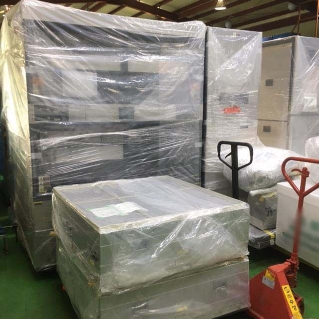


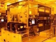







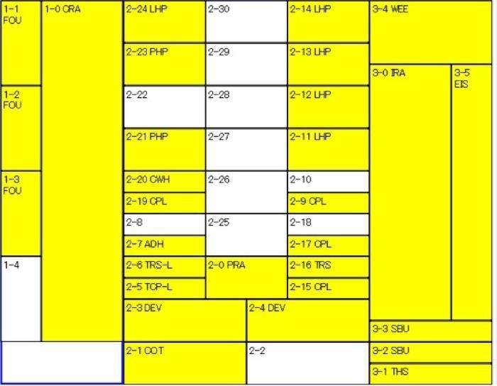



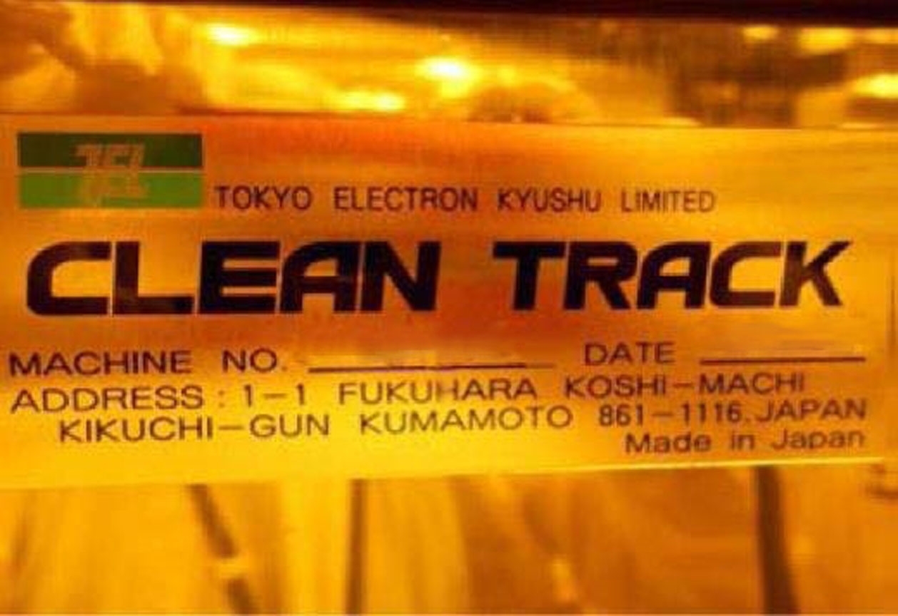

TEL / TOKYO ELECTRON Clean Track ACT 12 is a photoresist equipment designed to allow high-quality printing of sophisticated circuitry with high precision. This robust system is capable of printing extremely intricate line structures with minimal distortion and high accuracy. It has a track-width resolution of 350 nanometers and a layer-to-layer repeatability tolerance of less than 3 nanometers. The photoresist unit consists of a two-step process with spin-on resist and lithographic imaging. First, spin-on resist is applied to the substrate or wafer. This liquid resist is dispensed on to the wafer and then it is rotated at high speed in order to spread an even layer over the entire substrate. The resist must be applied with an extremely high level of precision and uniformity in order to achieve high-quality prints. Once the spin-on resist has been applied, the wafer is then exposed to a high-powered UV light source. This is where the lithographic imaging takes place. The device is able to precisely control the amount of light energy and exposure in order to produce a 'negative' image from the resist layer. The lithographic image is then used to print the desired circuit design. After the imaging process, a cascade of developer, rinsing, and oven steps are used to 'bake in' the design into the resist layer. The machine can process wafers up to 8-inches in diameter and can be set up for manual or automatic operation. The speed and accuracy of the clean track tool make it perfect for high-precision printing of intricate circuitry. The asset also allows for post processing to improve imaging resolution. This includes multiple resist layers, selective doping, laser cutting, and other advanced techniques. TEL Clean Track ACT 12 is a simple-to-use yet powerful photoresist model capable of producing sophisticated circuit designs with minimal deviation.
There are no reviews yet

