Used TEL / TOKYO ELECTRON Clean Track ACT 12 #9282380 for sale
URL successfully copied!
Tap to zoom


ID: 9282380
Wafer Size: 12"
Vintage: 2003
Coater / Developer system, 12"
Left to Right
FOUP carrier
(3) FOUP Loader uni-cassetes
(3) Main controllers
(2) Thermo controllers
(2) Fire system boxes
PRB
CSB
IFB
Main system:
Main frame with system controller
Carrier station
FOUP Cassette
(3) Cassettes
Uni-cassette system
Coater unit:
(6) Dispense nozzles
With temperature control line
MILLIPORE RDS Pump
Rinse nozzle: EBR / Back rinse / Solvent bath
Rinse system: (2) Buffer tank systems (3-Liters)
Degassing system
Programmable side rinse
PR Nozzle
(6) Bottles
Thinner supply: CCSS
AMC Suck-back valve
Direct drain
Developer unit:
H Nozzle:
Stream nozzles for DI rinse
2-Points for back side rinse
Developer systems: (2) Buffer tank systems (3 Liters)
Developer supply: CCSS
Degassing system
Developer temperature control system
Direct drain
NIKON SF130 Wafer stage
Adhesion units:
100% Sealing closed chamber (Built-in hot plate)
HMDS Tank with float sensor
HMDS Supply
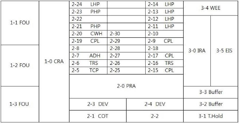
(5) Low temperature Hot Plates (LHP)
(4) Chill Plates (CPL)
(2) Precision chilling Hot Plates (PHP)
TCP Unit
(2) TRS Units
Wafer Edge Exposure (WEE) unit
I-line UV Sensor
Chemical cabinet 1: HNDS and Solvent supply system
Chemical cabinet 2: DEV Solution and DIW supply system
SHINWA Series ESA-8 Humidity controller
Temperature Control Units (TCU)
AC Power box
2003 vintage.
TEL / TOKYO ELECTRON Clean Track ACT 12 is a photoresist (PR) equipment designed to make the production of semiconductor devices faster and more efficient. It is a highly advanced solution that is used to create the intricate patterns for the transfer of electrical signals on a silicon wafer surface. The system consists of several different components, some of which are designed to optimize the accuracy of the patterns and guarantee a very high yield. The first is TEL clean track ETCH unit. This machine uses a combination of dry etching and chemical etching to make sure that the wafer is correctly patterned. There is also an advanced lithography tool for accurately setting up the PR asset. The model also includes the AC-magnet equipment for controlling the speed of the PR layers and optimizing the electronic data transfer. This system is also designed to reduce or eliminate any flaws in the production process. TEL Clean Track ACT 12 is very reliable and has several built-in safety systems. One of these is the Clean-Track process monitoring unit. This machine ensures that each process step is monitored and any errors can be corrected. The tool also has an in-line mirror asset that is used for real-time surface monitoring to make sure that the PR layers are applied correctly. Another important feature of TOKYO ELECTRON Clean Track ACT 12 is its ability to quickly change the parameters of the PR layers according to the needs of the products being produced. This allows for a high degree of flexibility and faster production time. Finally, the model is also capable of automatically detecting any defects during the production process. This allows for a more comprehensive and faster quality control and for the quick resolution of any errors. Overall, Clean Track ACT 12 is a highly advanced and efficient photoresist equipment. Its combination of innovative features and dependability make it the ideal choice for the quick and accurate production of semiconductor devices.
There are no reviews yet