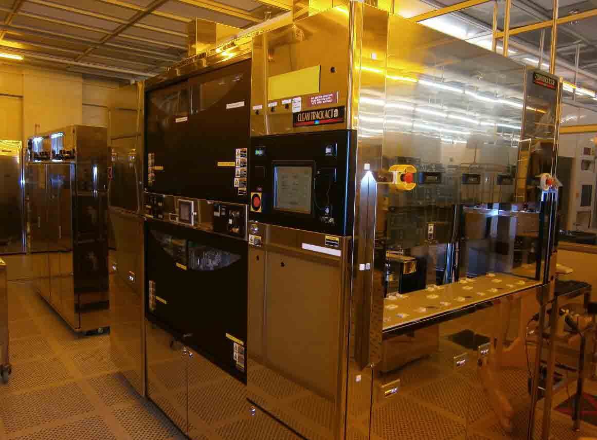
Used TEL / TOKYO ELECTRON Clean Track ACT 8 #293633988 for sale
It looks like this item has already been sold. Check similar products below or contact us and our experienced team will find it for you.
Tap to zoom


Sold
ID: 293633988
(2) Coater / (2) Developer system
SOD Track
Coater cup
Cup rinse
Dispense Detect System (DDS)
Spinfil dispense system
Spinfil drain line
HC-100 PCS Pump
LHP High exhaust
Exhaust interlock.
TEL / TOKYO ELECTRON ACT 8 is a photoresist equipment designed for producing highly accurate circuit patterns on semiconductor wafers. The system uses light exposure to selectively apply and remove a photoresist from the wafer's surface. Through specialized and sophisticated exposure and developing processes, the unit is able to produce precise, high-resolution patterns with a minimum linewidth of 8 nanometers. TEL ACT 8 machine consists of an exposure head, wafer handler and a stepper stage. The exposure head serves as a light source and contains a laser diode that emits laser light with wavelengths up to 248 nm. Through the stepper stage, the exposure head is able to move horizontally and vertically, allowing for accurate exposure control. The exposure head can be adjusted to support a variety of exposure processes, including single-point or multi-point laser exposure and scan exposure. The wafer handler delivers the wafer to the stepper stage and collects it after exposure. It also enables the user to perform wafer orientation, substrate exchange and wafer alignment. In addition, the tool supports a variety of substrates, including silicon and glass chips. The asset is designed to provide a high level of accuracy, uniformity and reproducibility, as well as flexibility in handling a wide range of materials. Using the model, a number of exposure techniques can be employed, including dynamic exposure optimization, applying exposure multiple times, and compensating for spherical aberration. TOKYO ELECTRON ACT 8 also comes with a suite of control software and hardware tools to help users achieve the desired quality and resolution in the circuit patterns. It includes exposure pattern analysis software and automatic pattern matching functions that enable users to adjust the photoresist requirements and exposure conditions in order to achieve the desired precision and accuracy in the pattern. Overall, TOKYO ELECTRON ACT 8 is a powerful photoresist equipment offering a high level of accuracy and uniformity in producing circuit patterns on semiconductor wafers. Its specialized exposure and developing processes enable highly precise and reproducible circuit patterns of minimum 8-nanometer linewidth. In addition, its suite of control software and hardware tools make it easy to use and customize for various applications.
There are no reviews yet