Used TEL / TOKYO ELECTRON Clean Track ACT 8 #293767233 for sale
URL successfully copied!
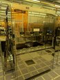
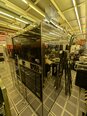
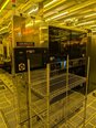
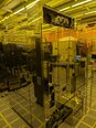




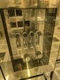



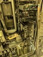
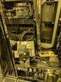
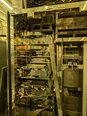
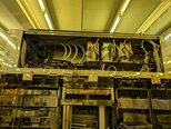
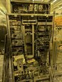

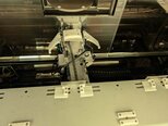
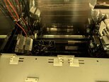


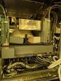
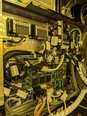
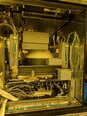
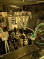
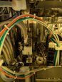
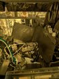
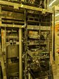
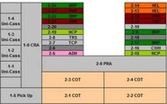


Tap to zoom
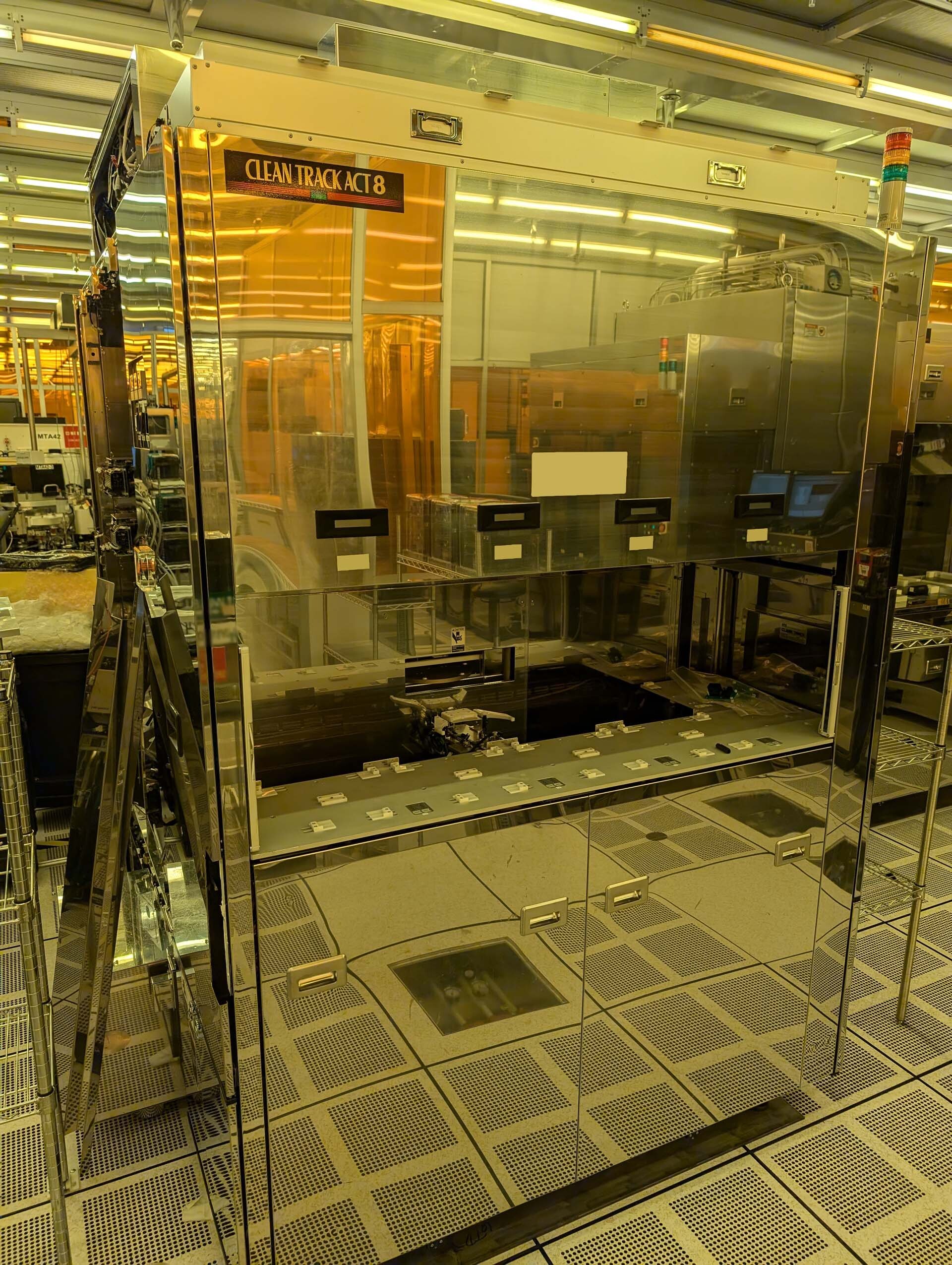

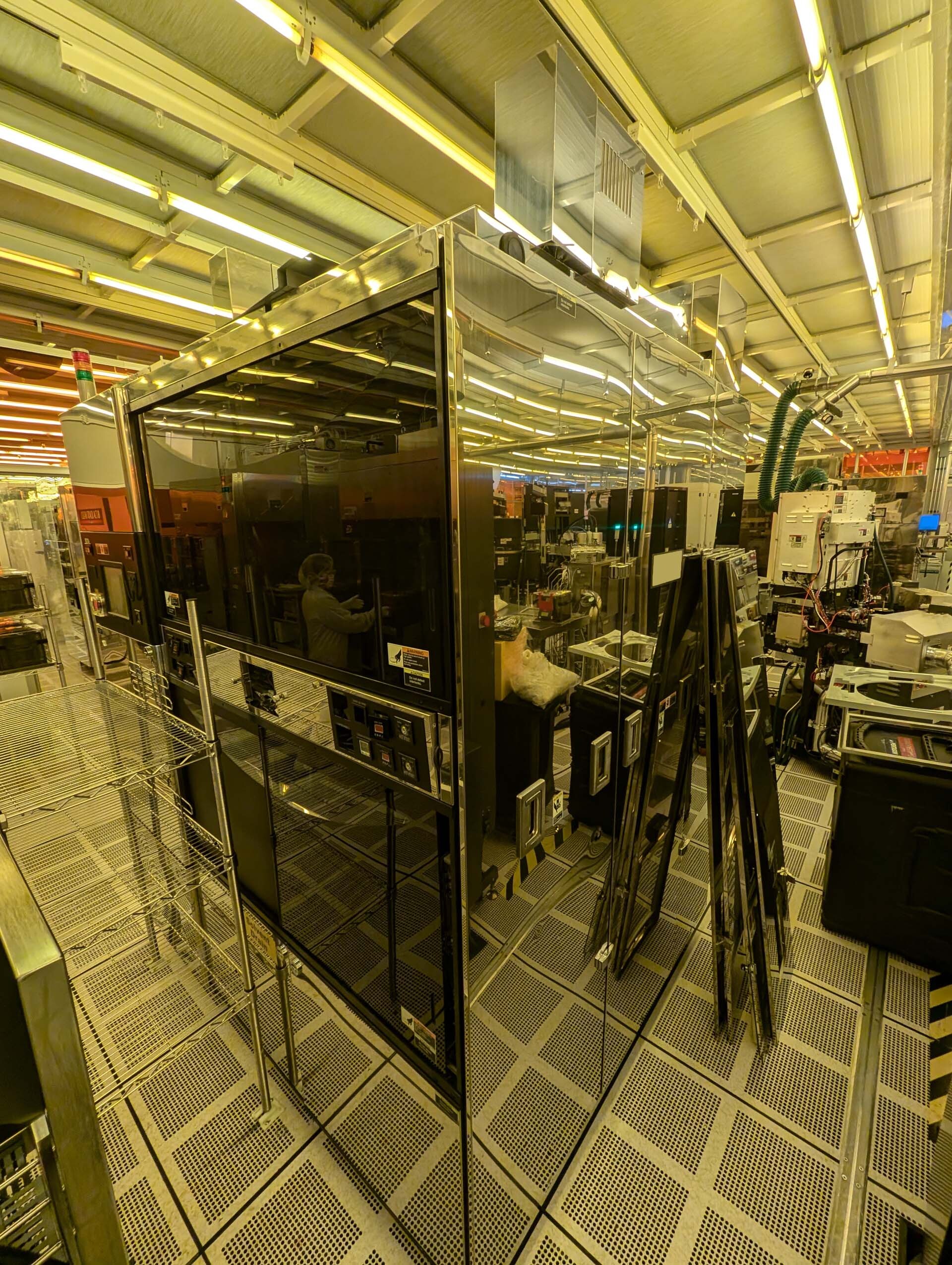
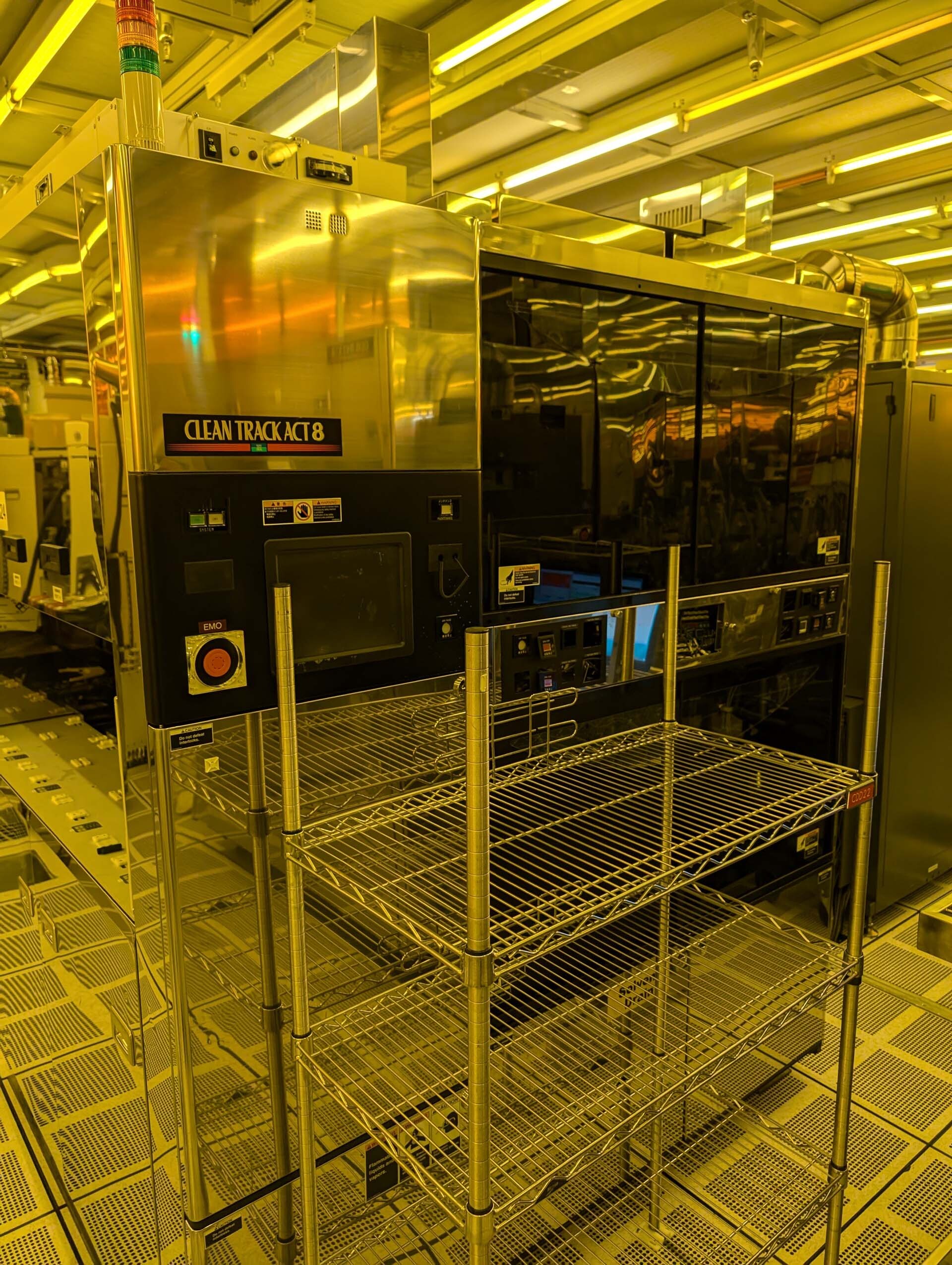
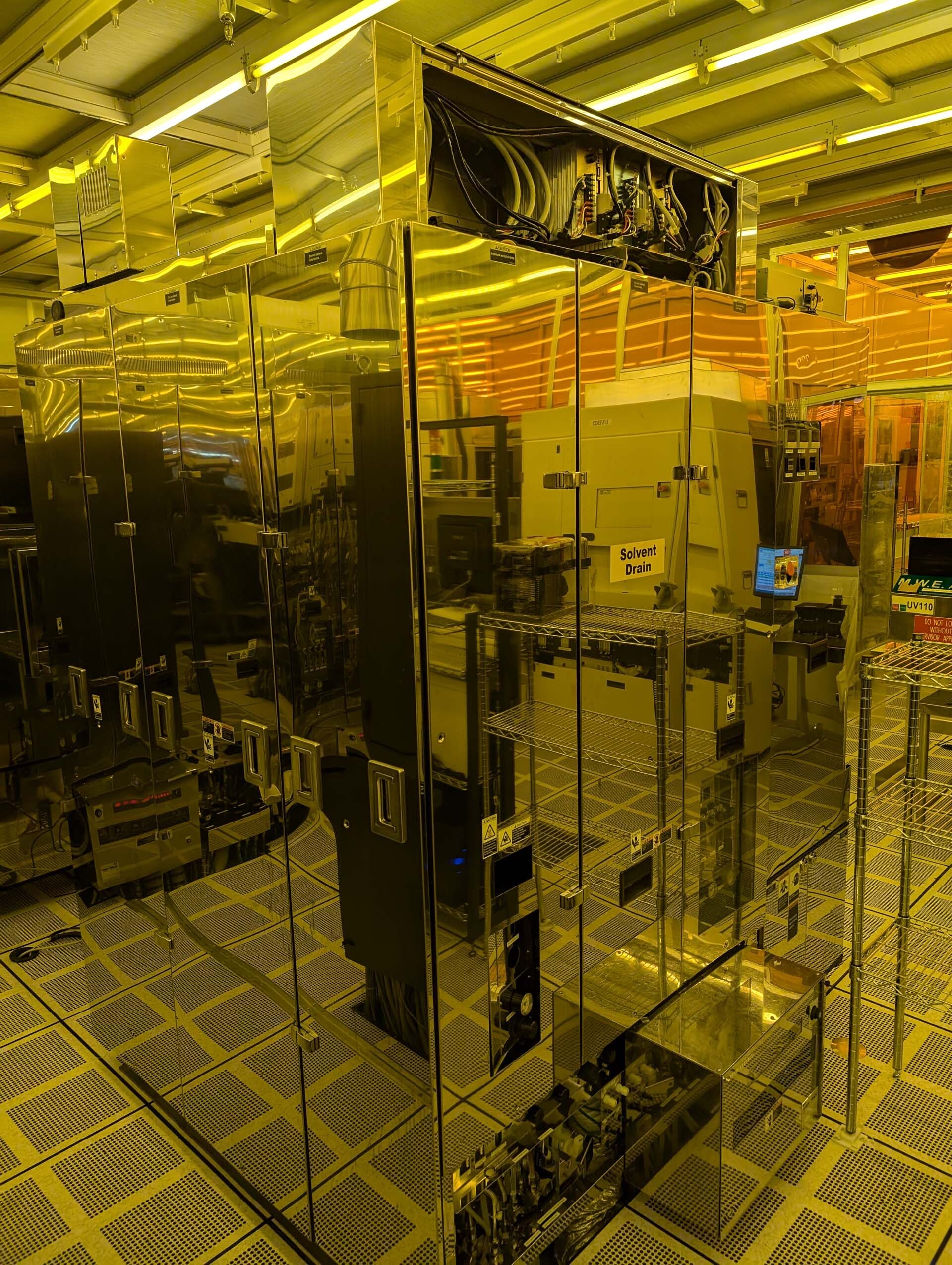
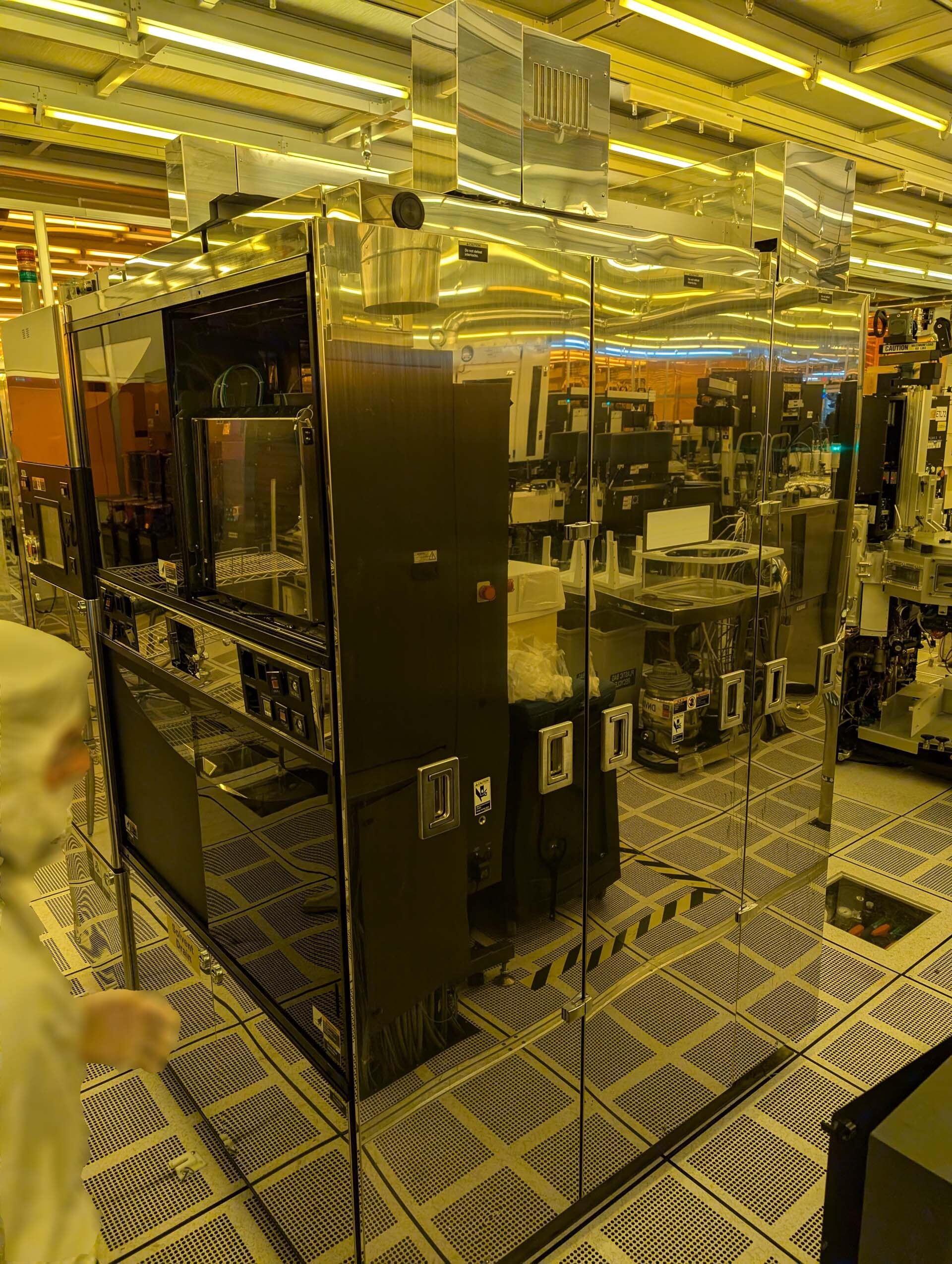
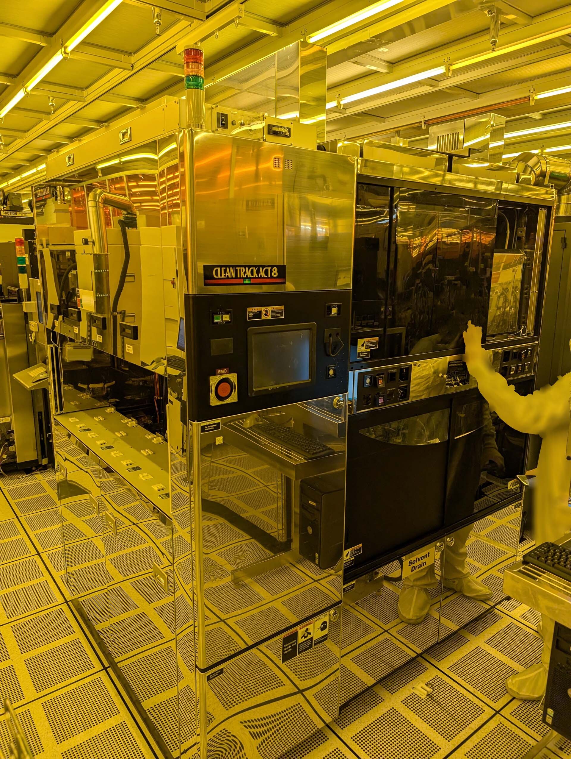
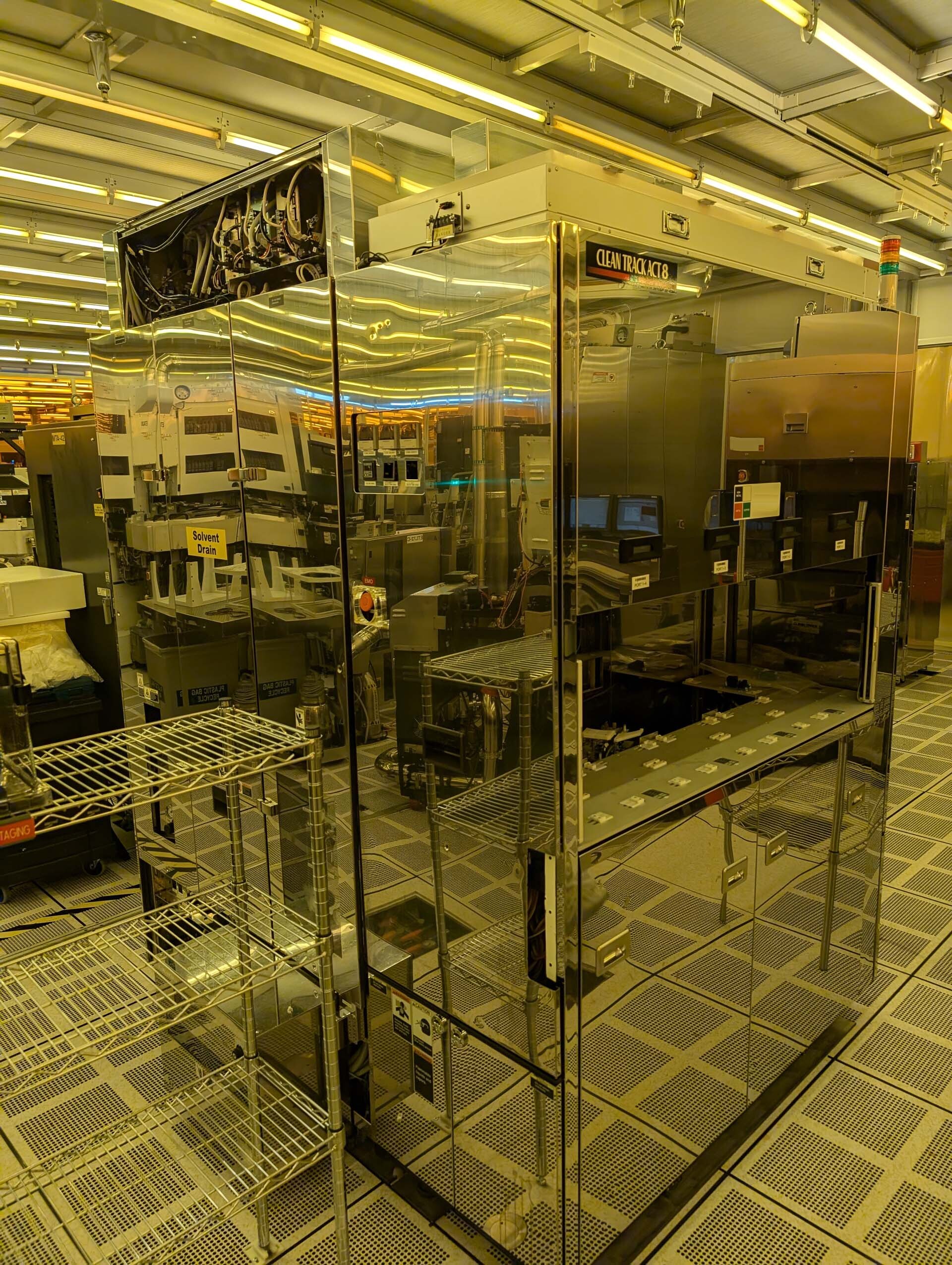
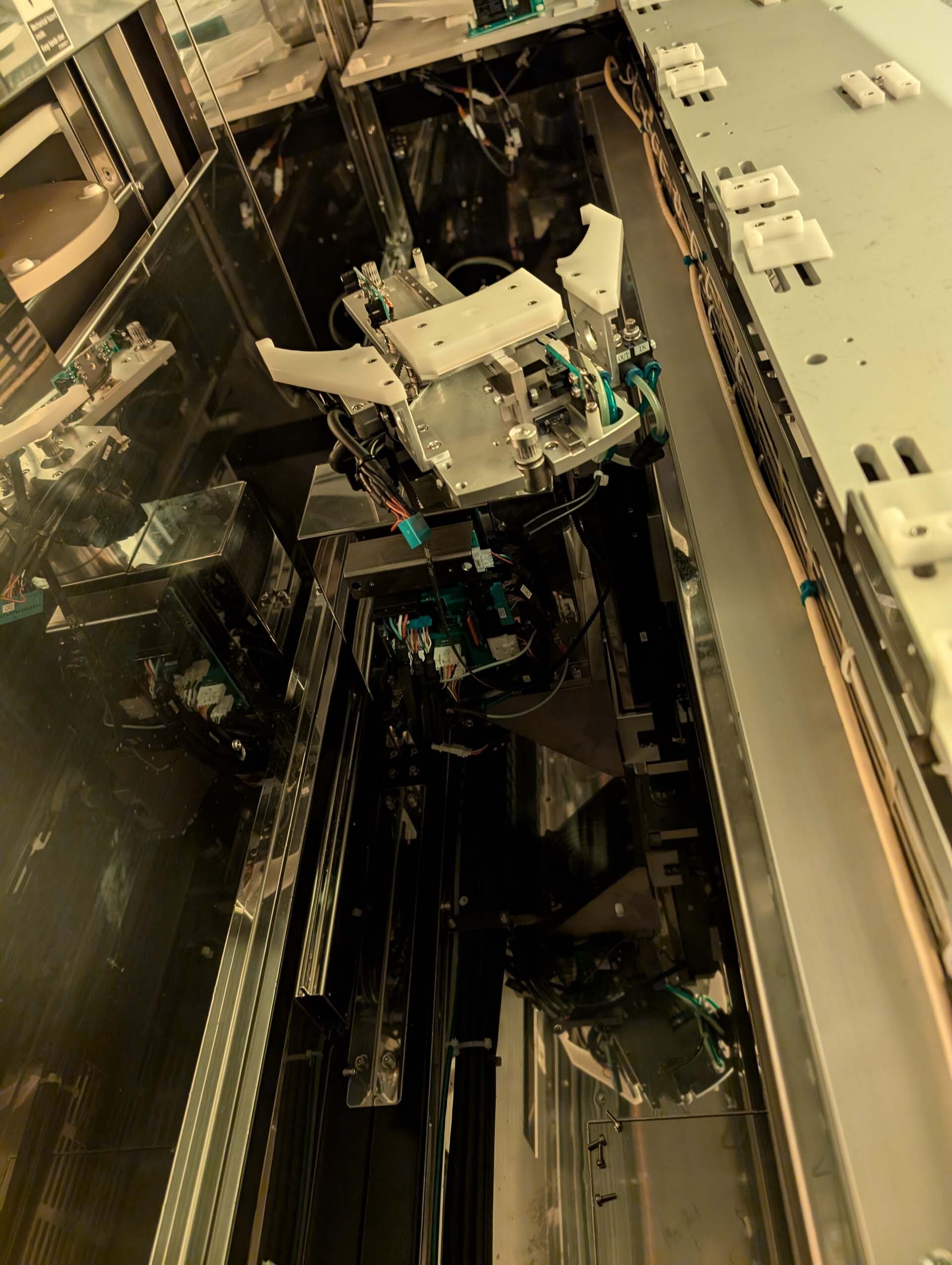
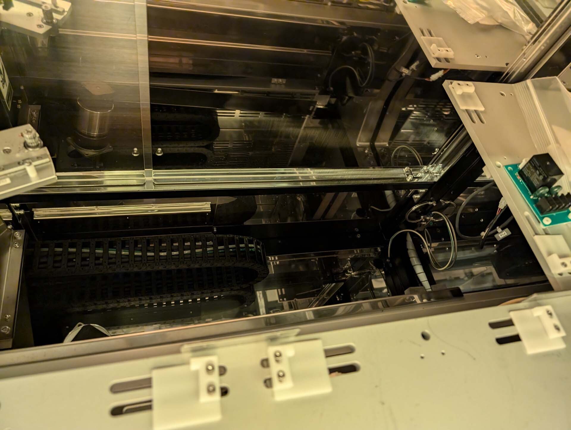
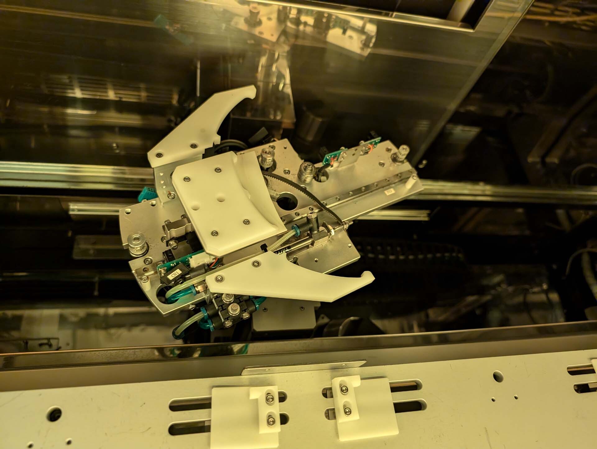
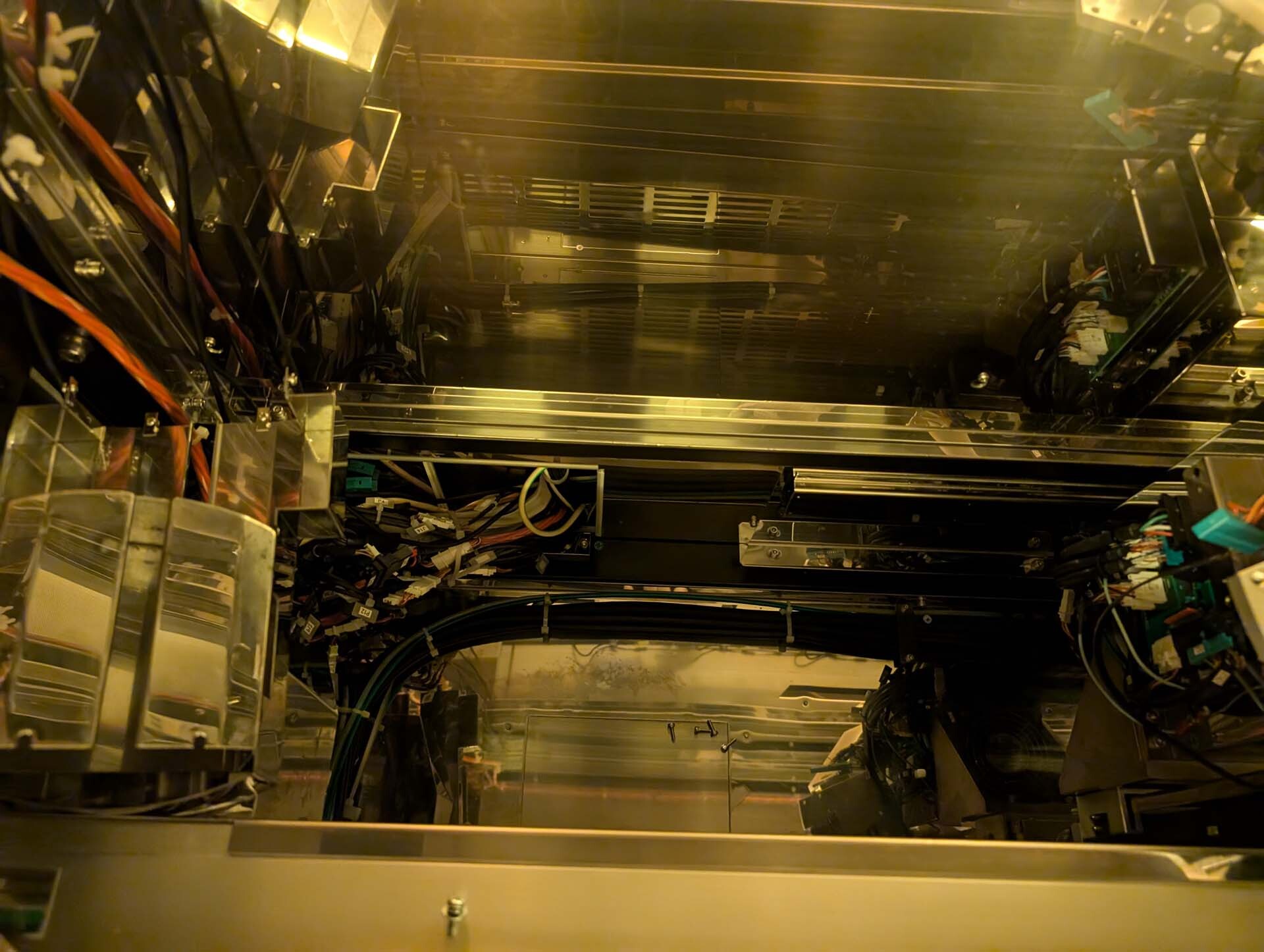
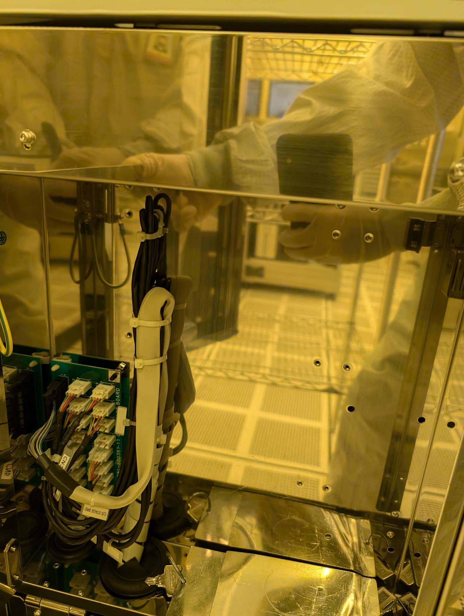
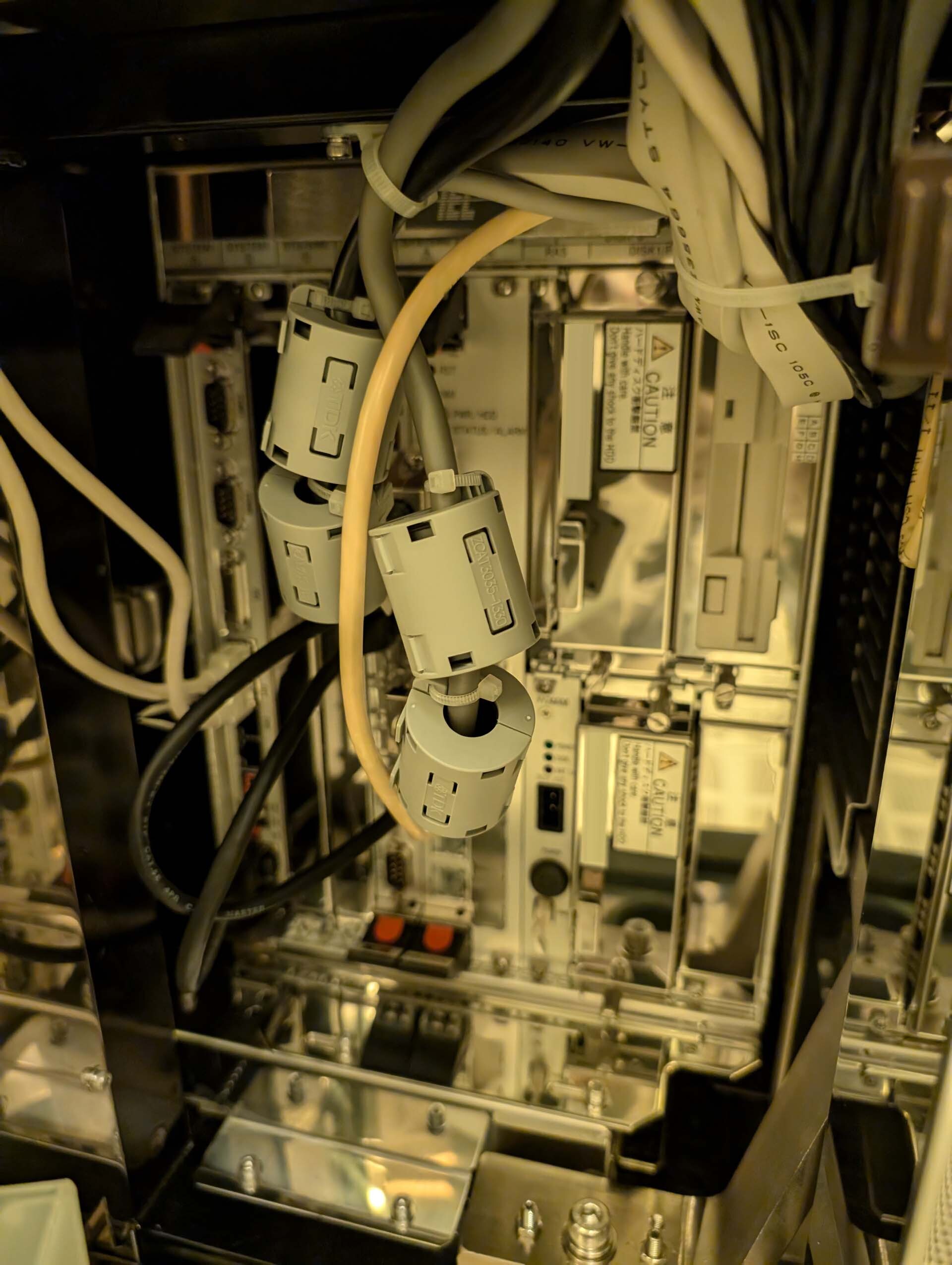
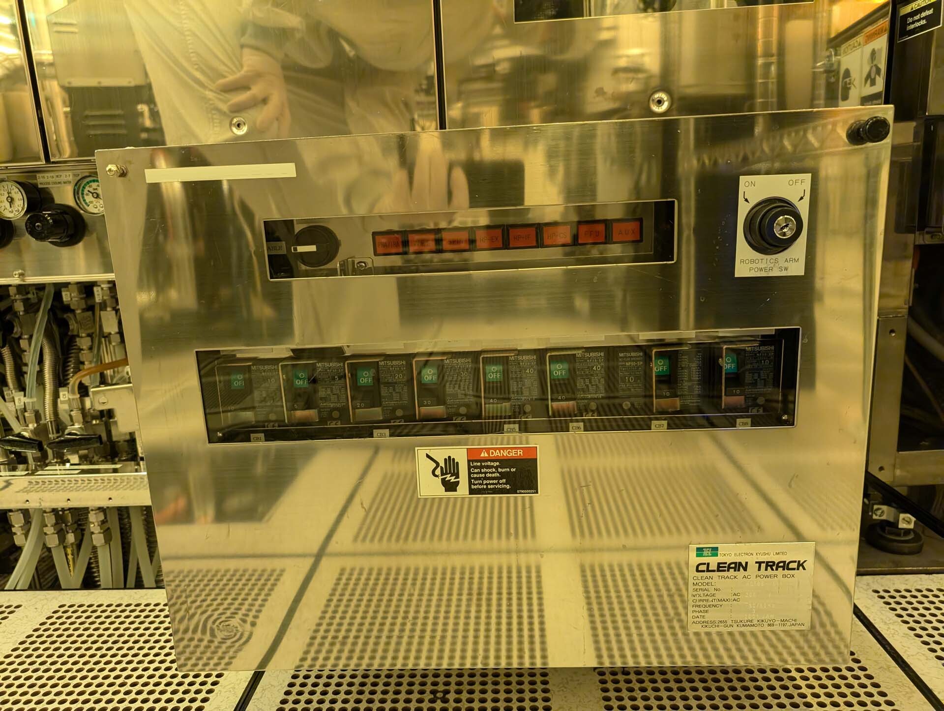
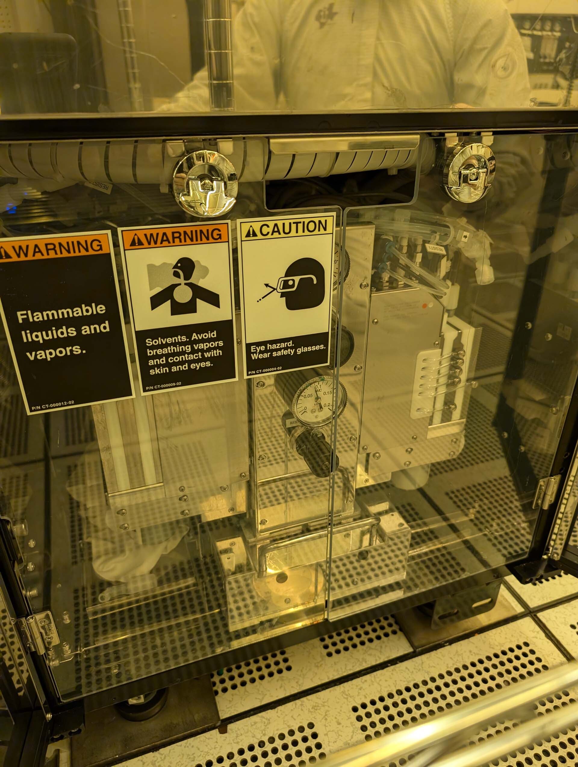
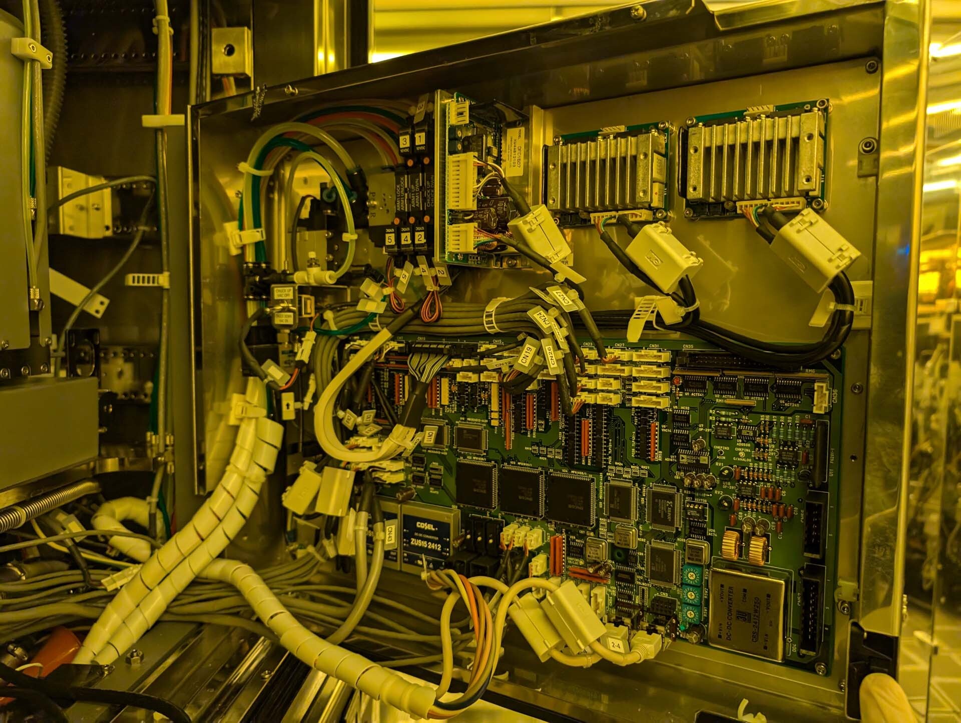
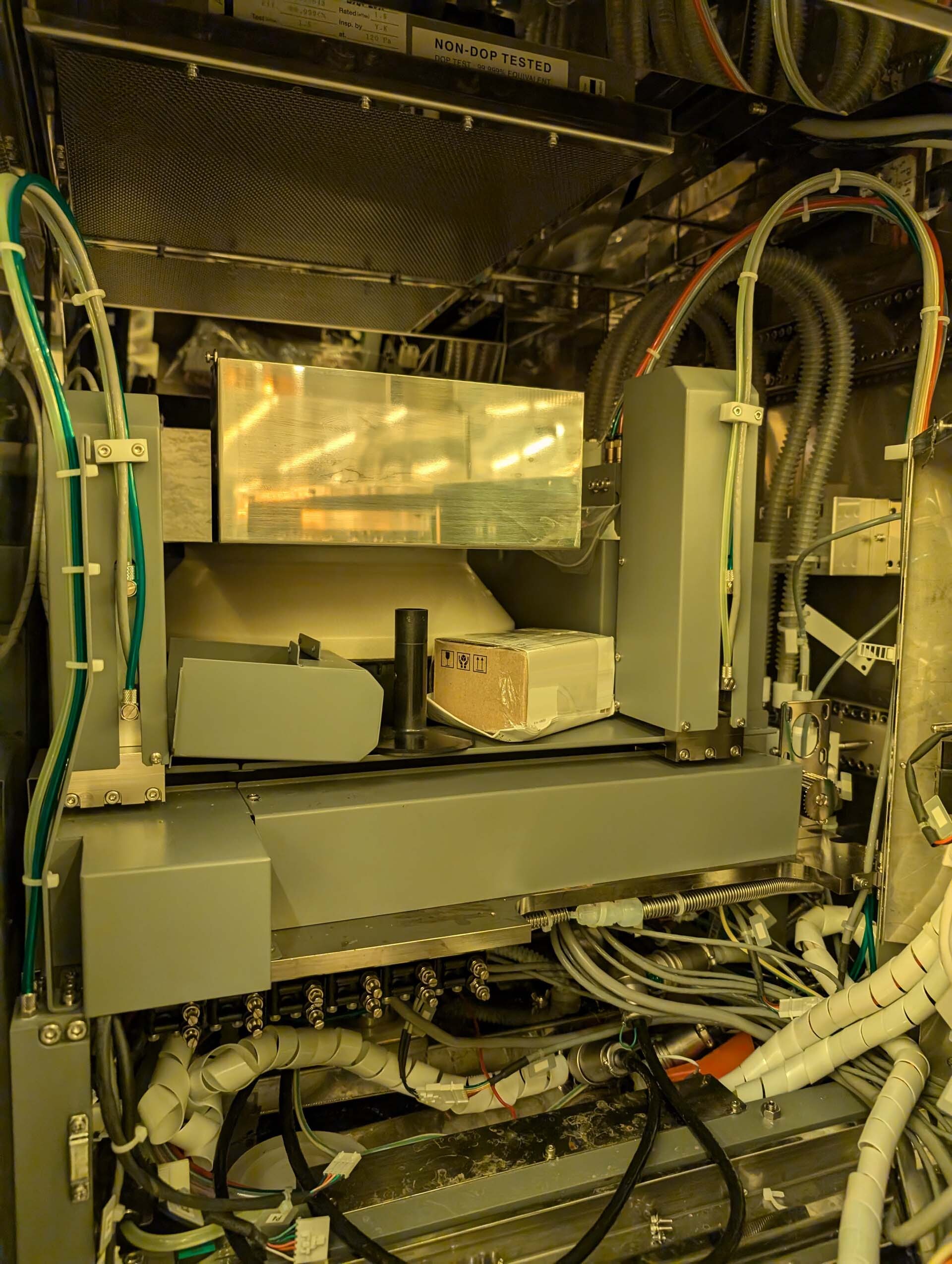
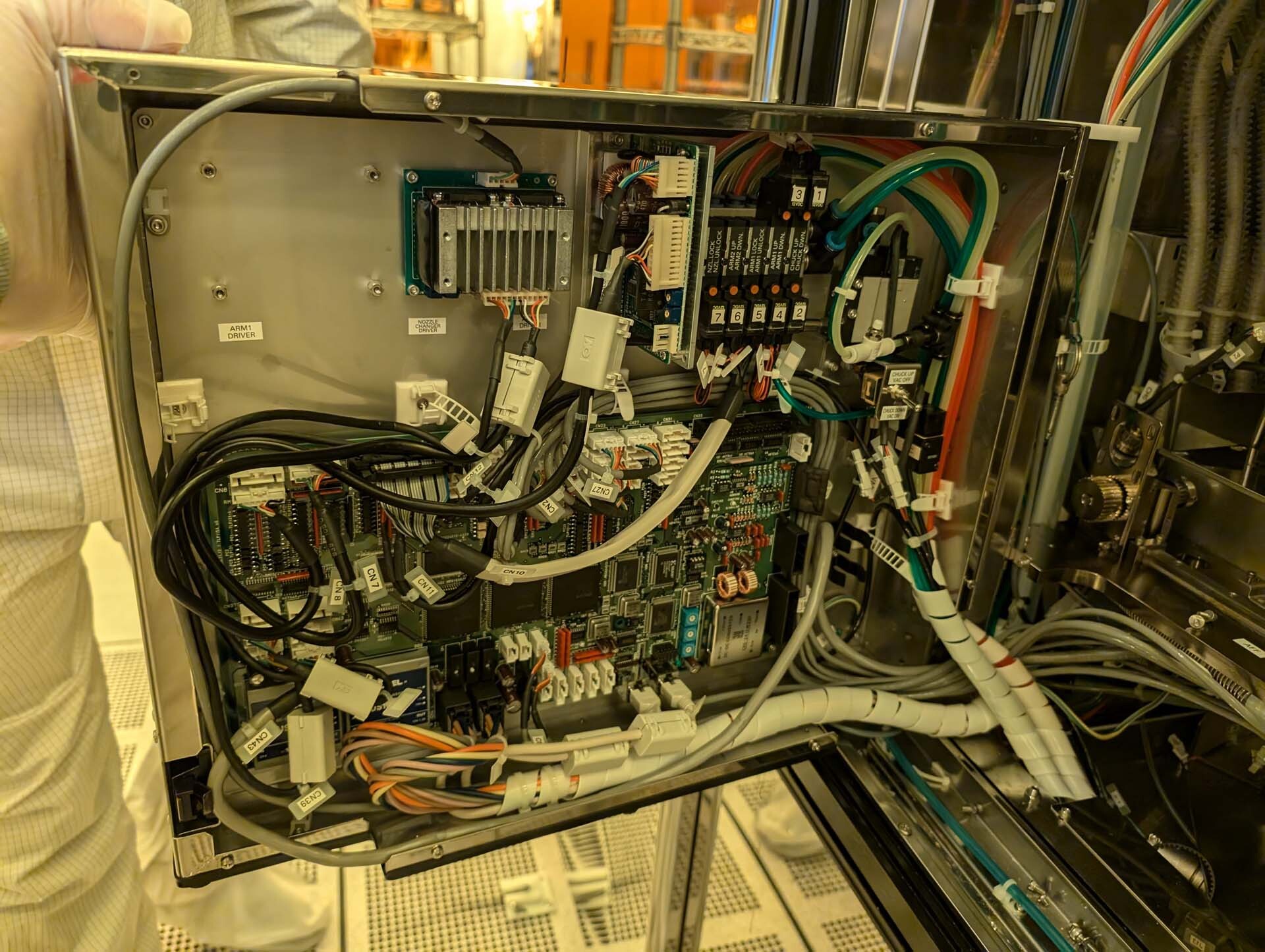
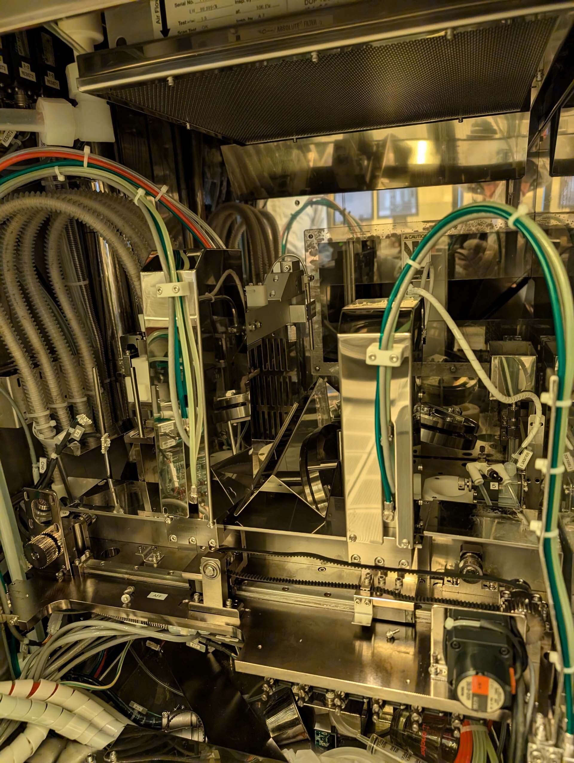
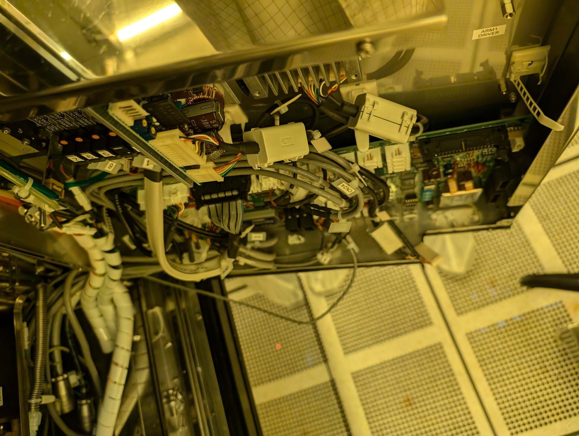
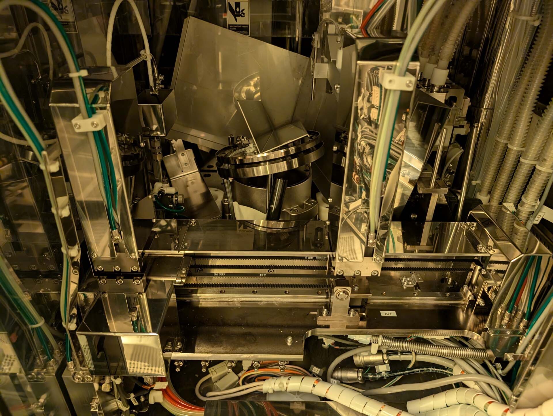
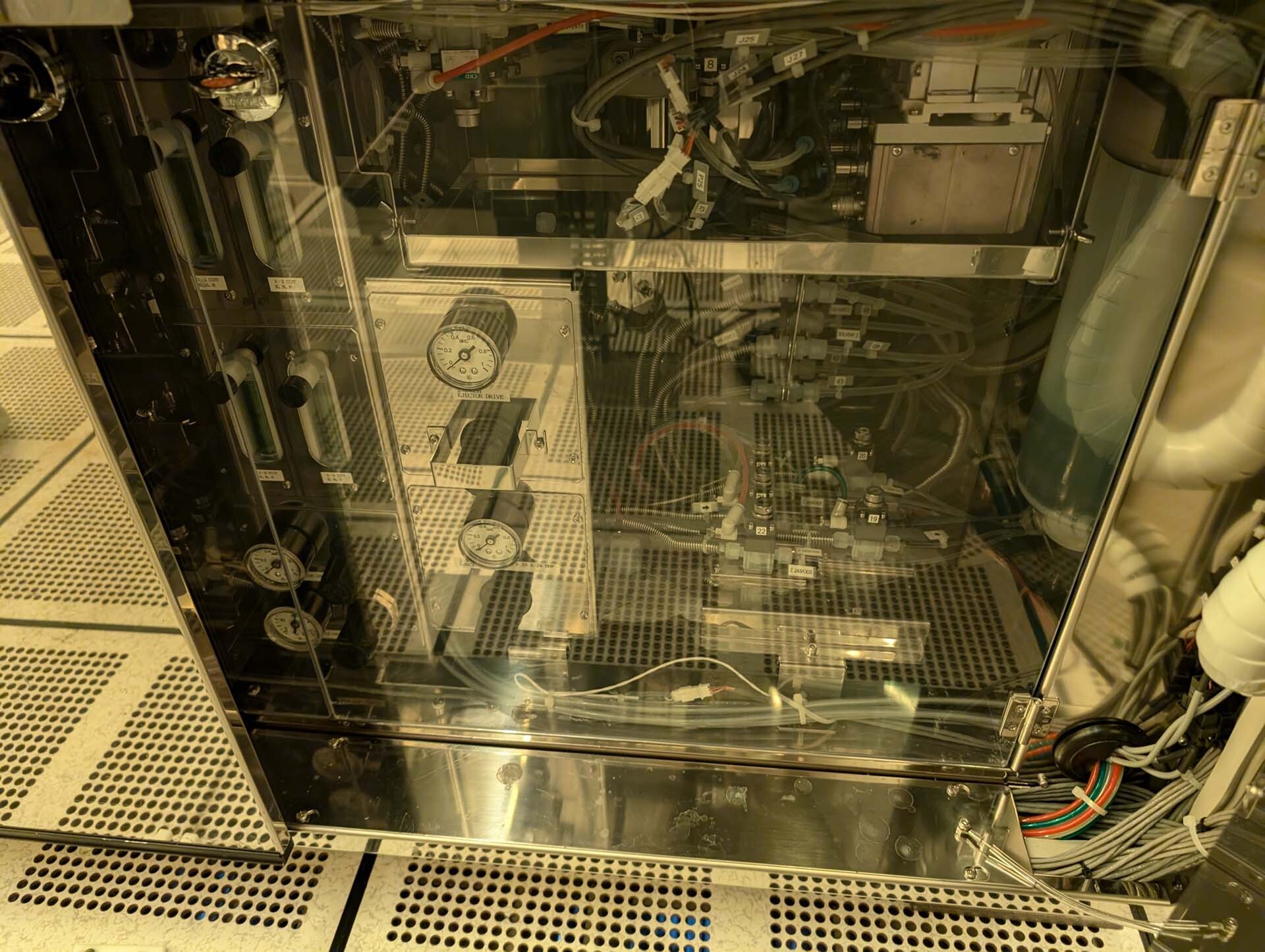
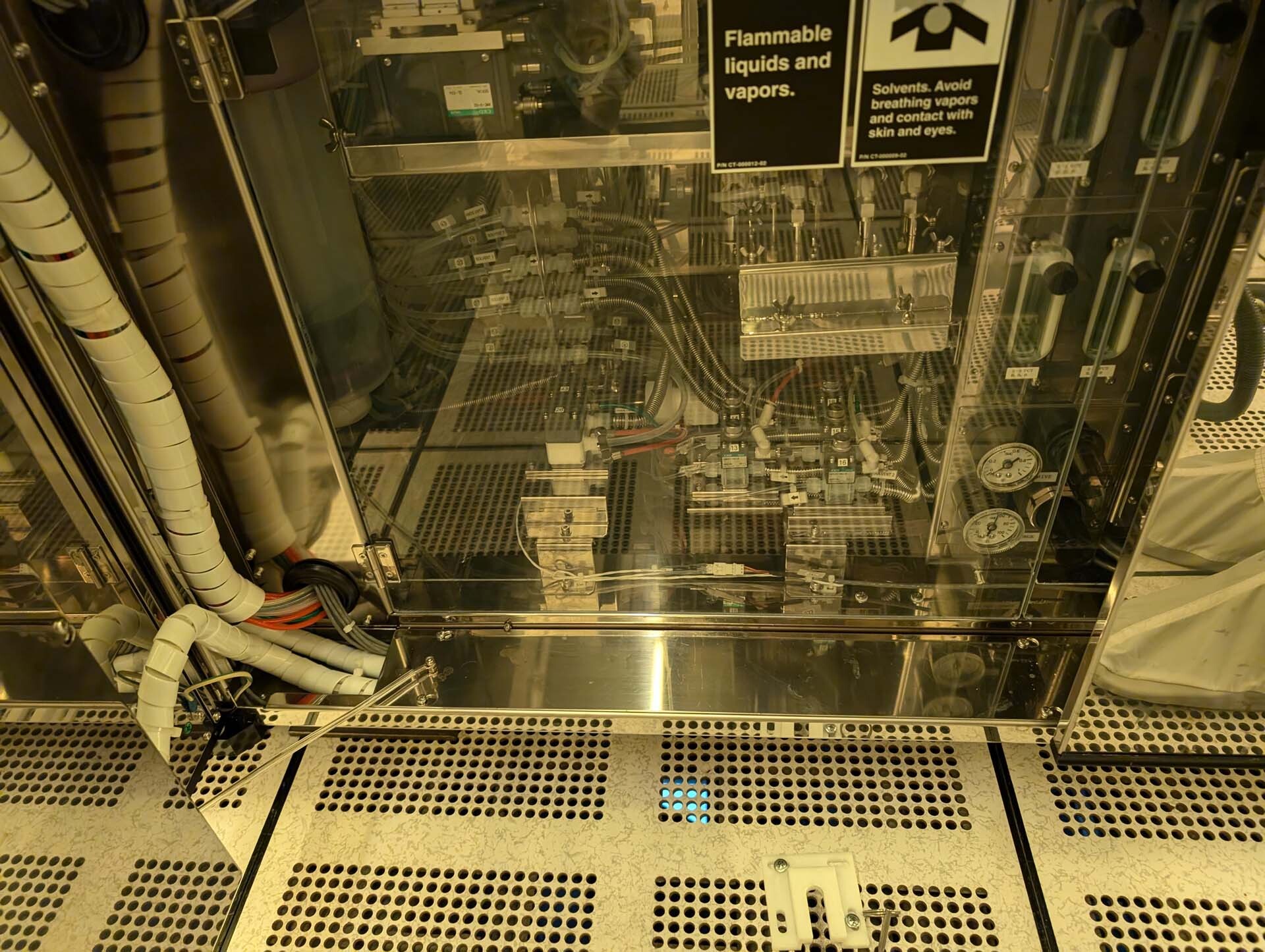
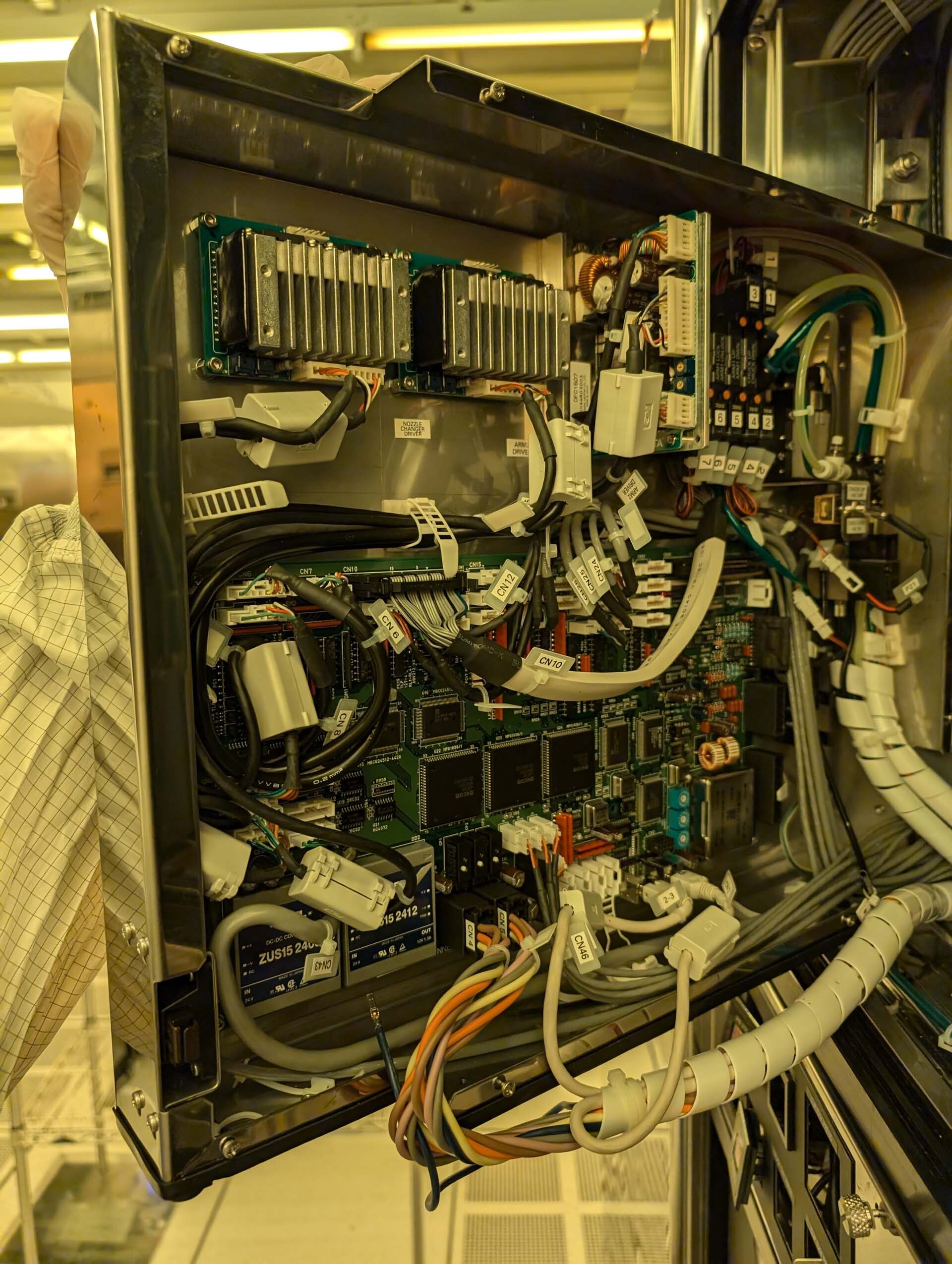
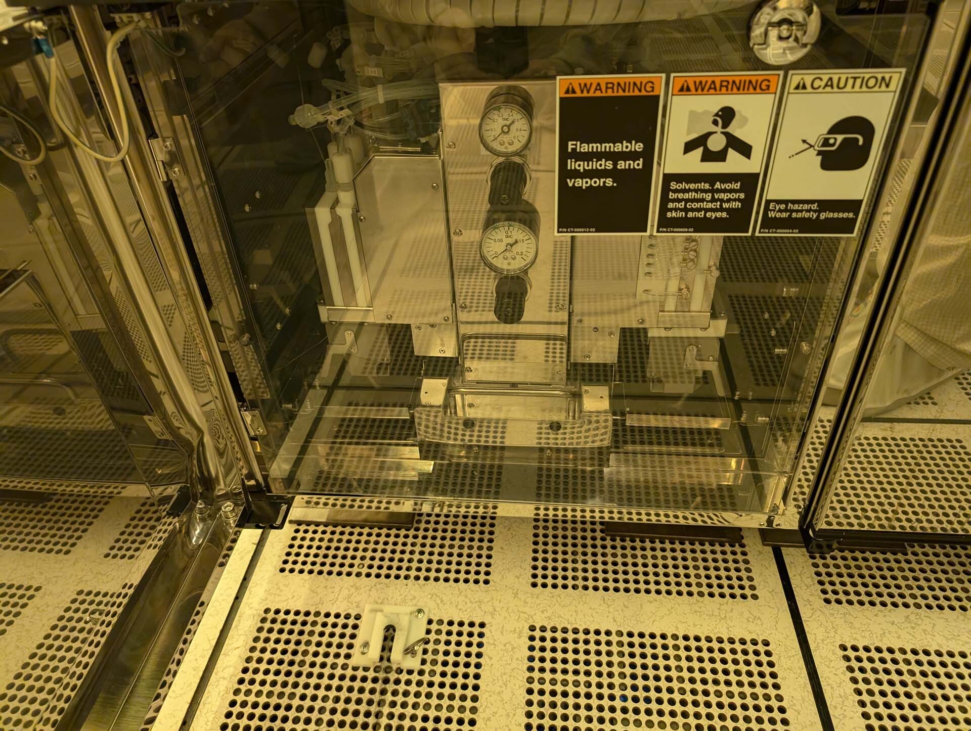
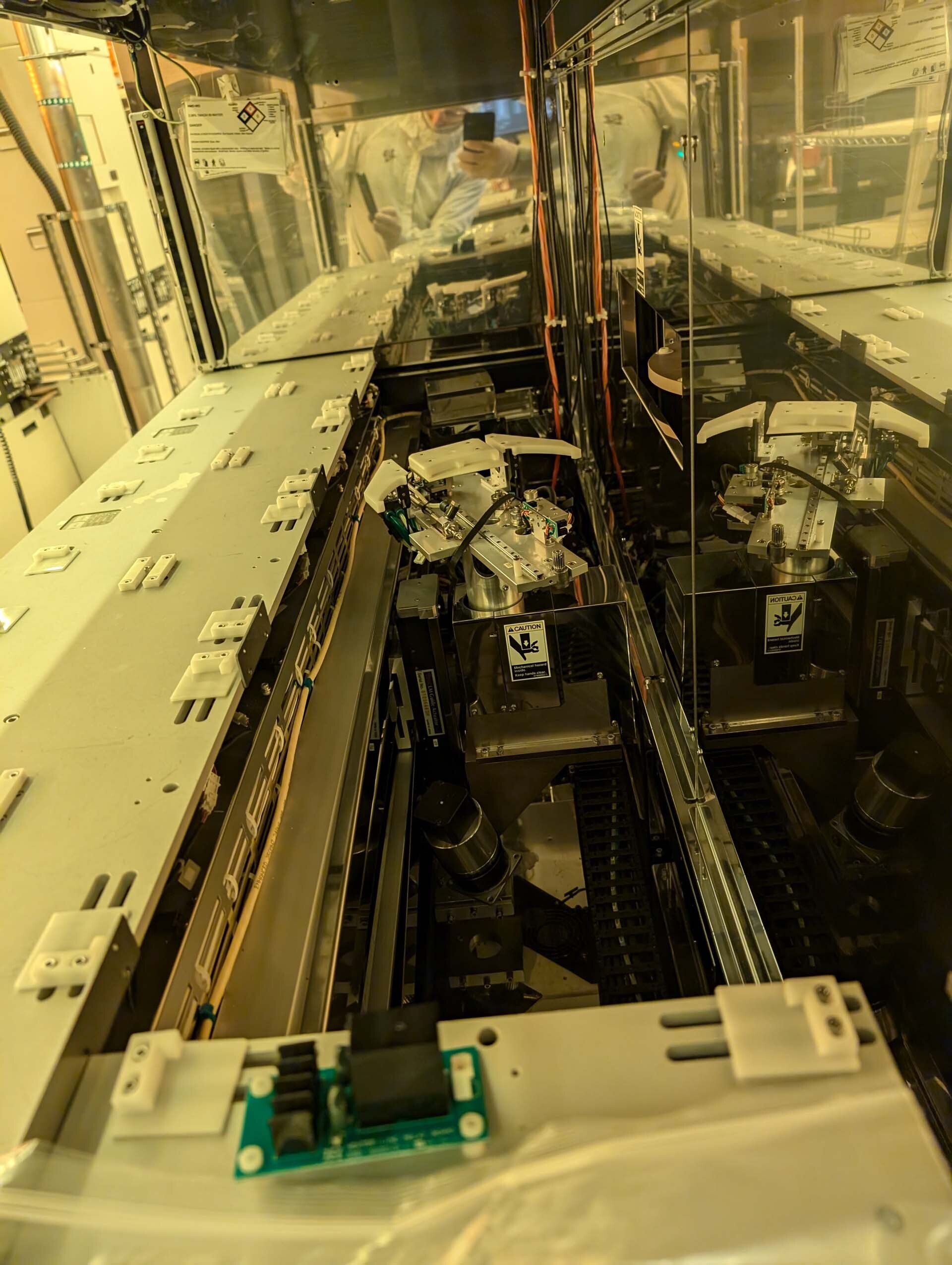
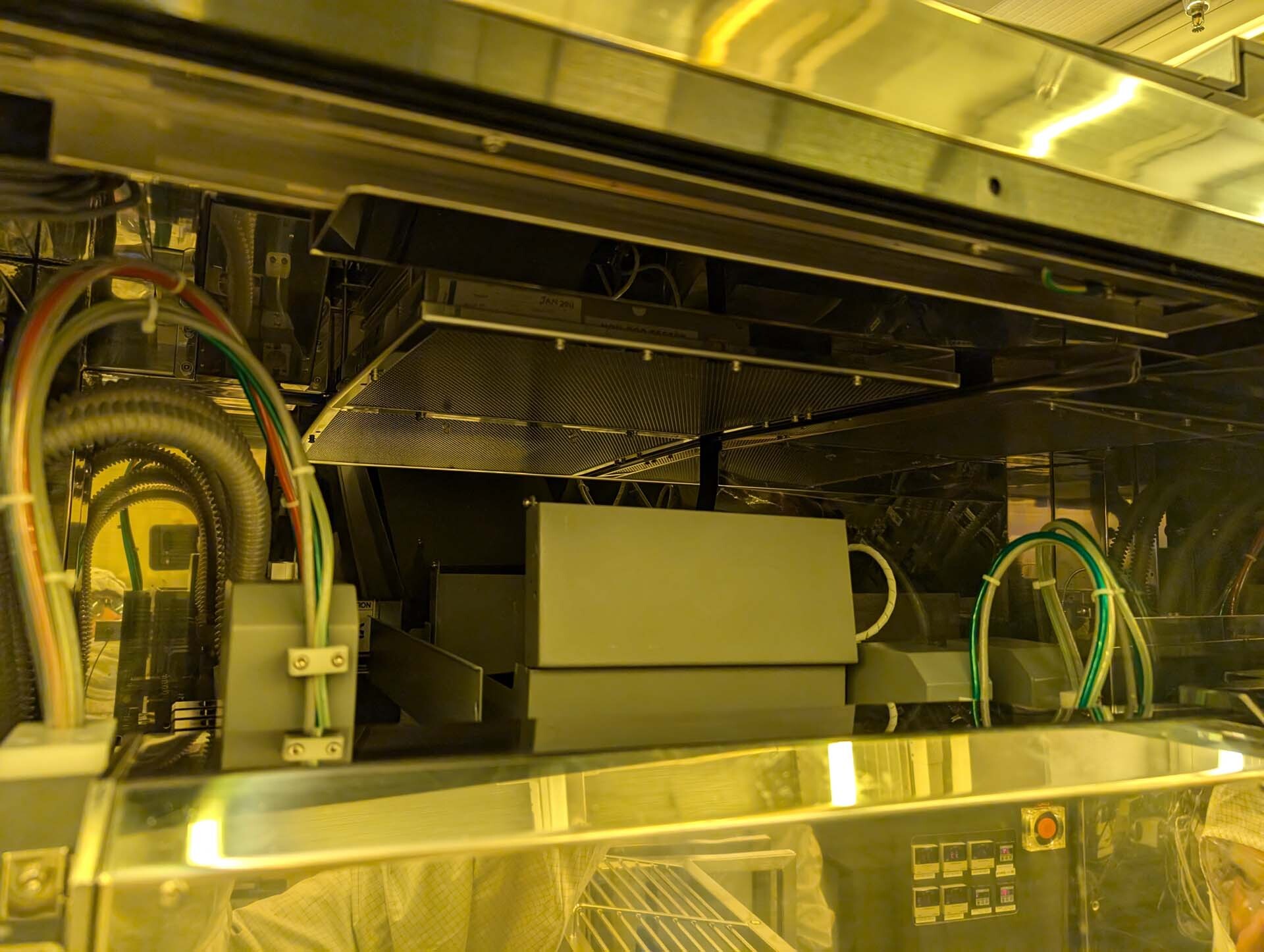
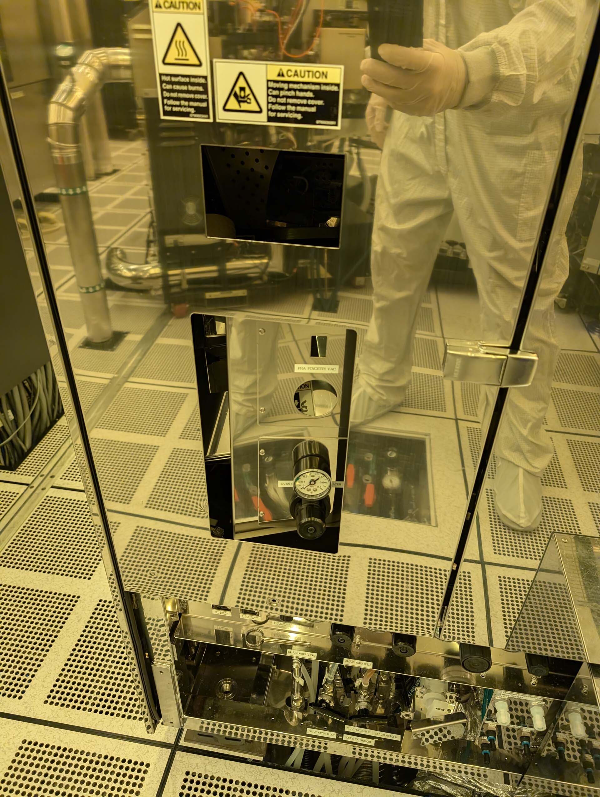
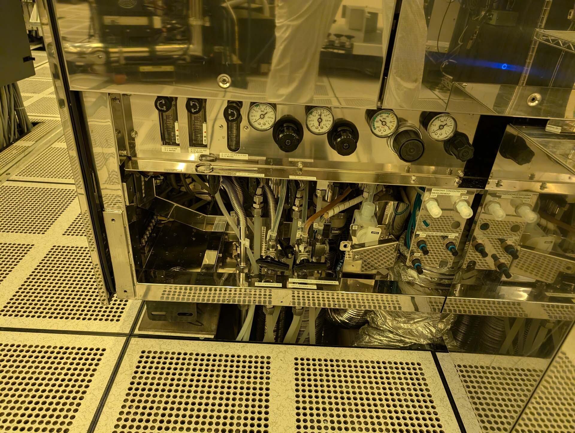
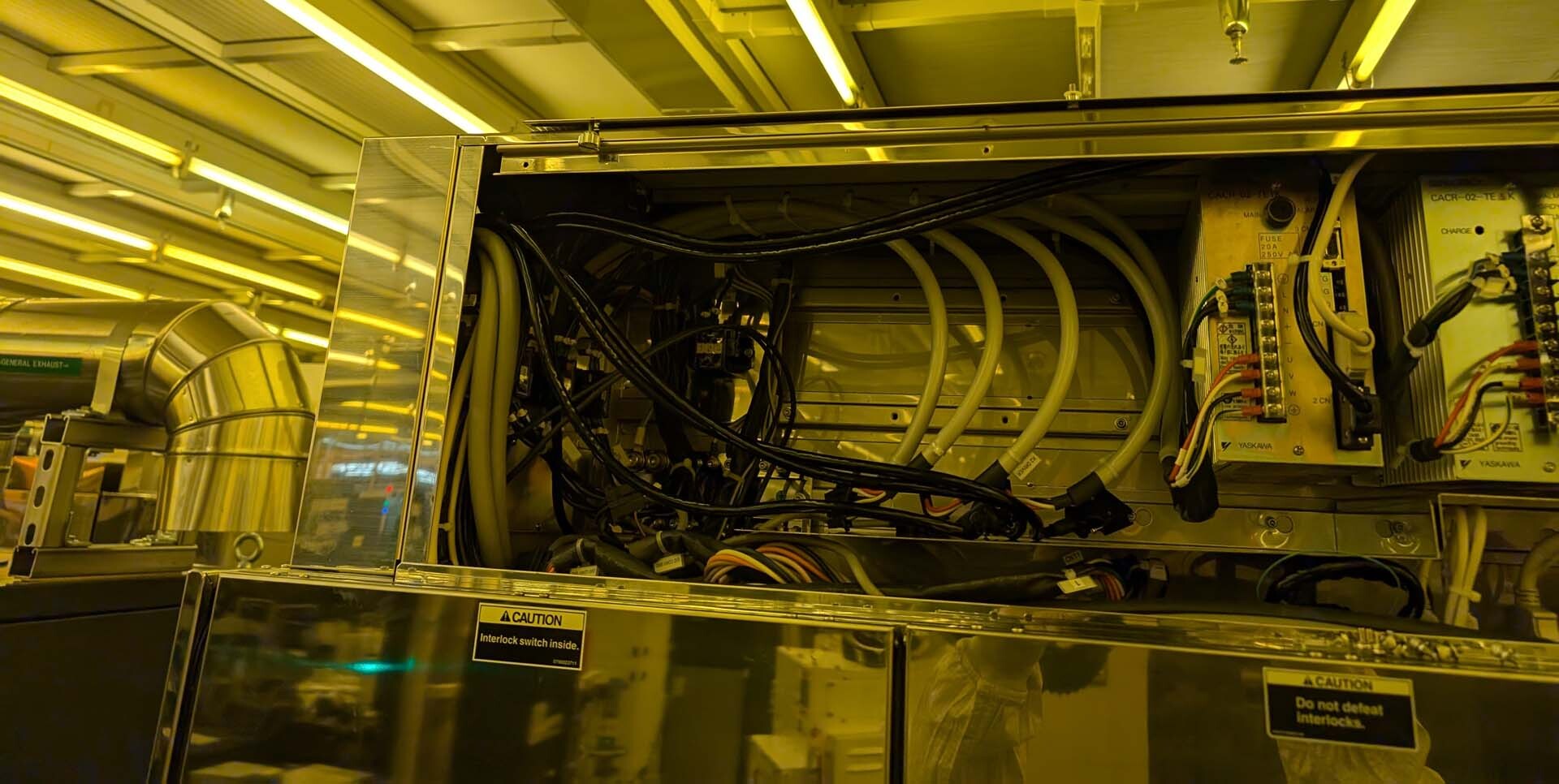
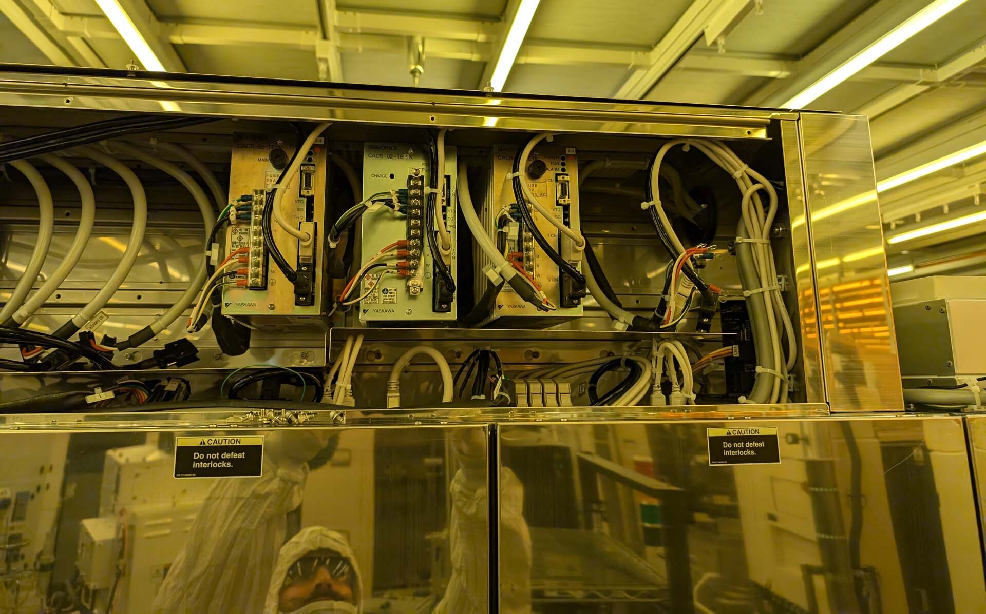
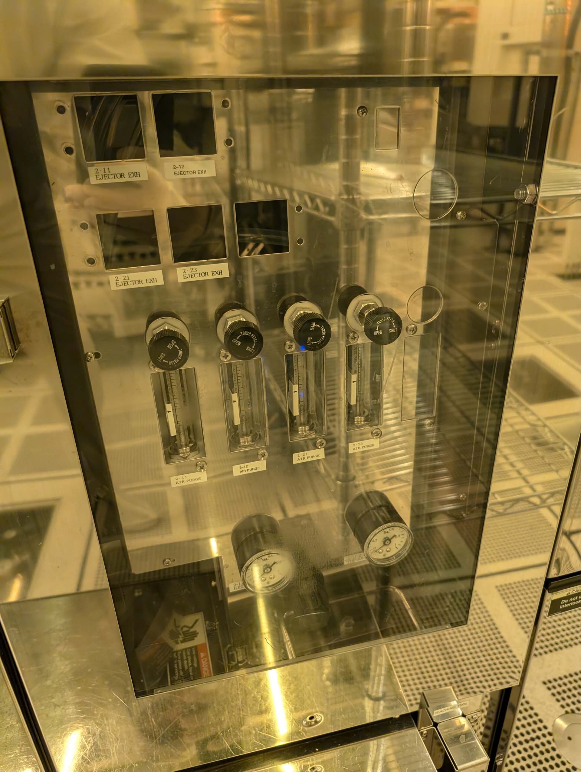
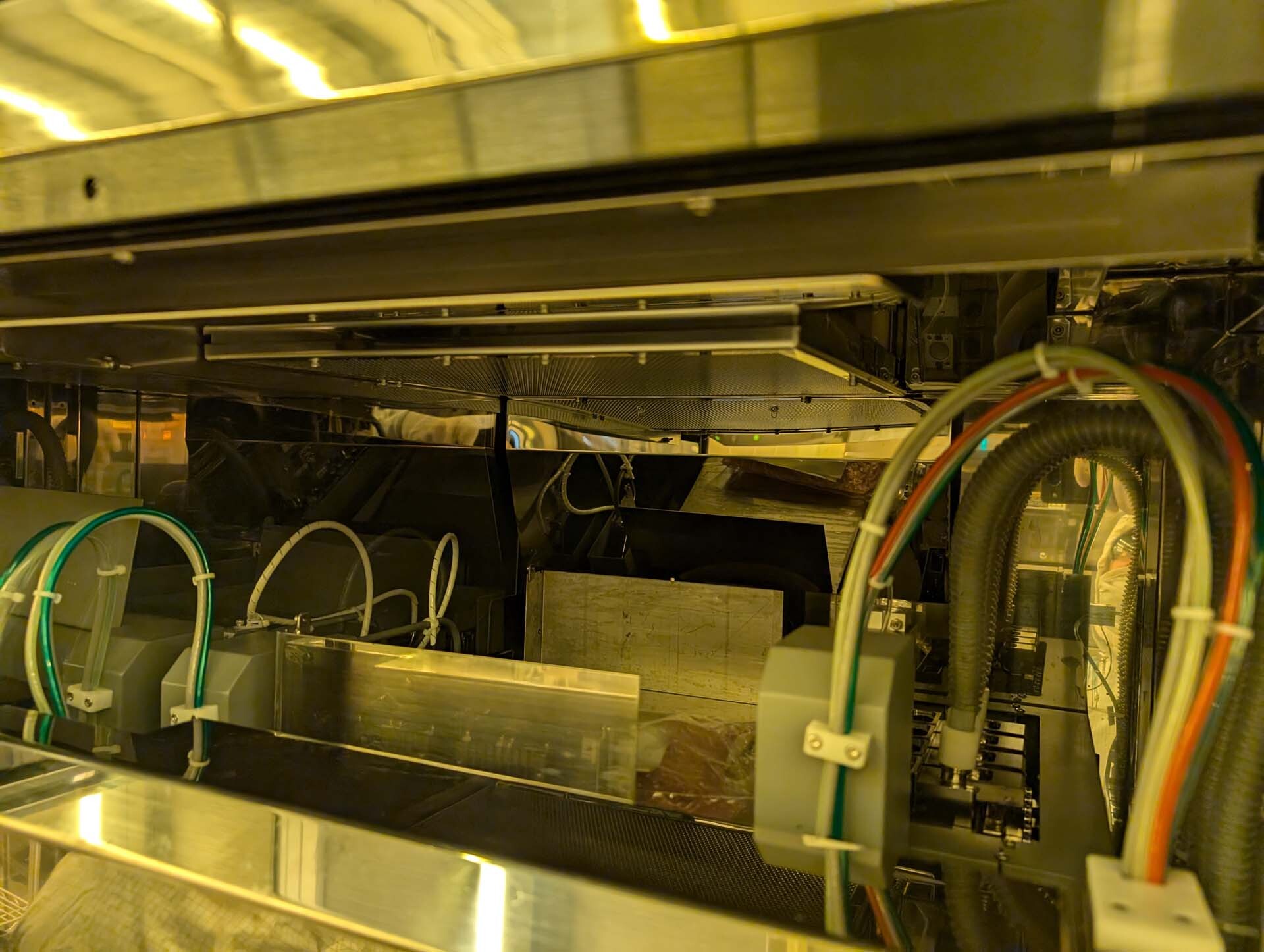
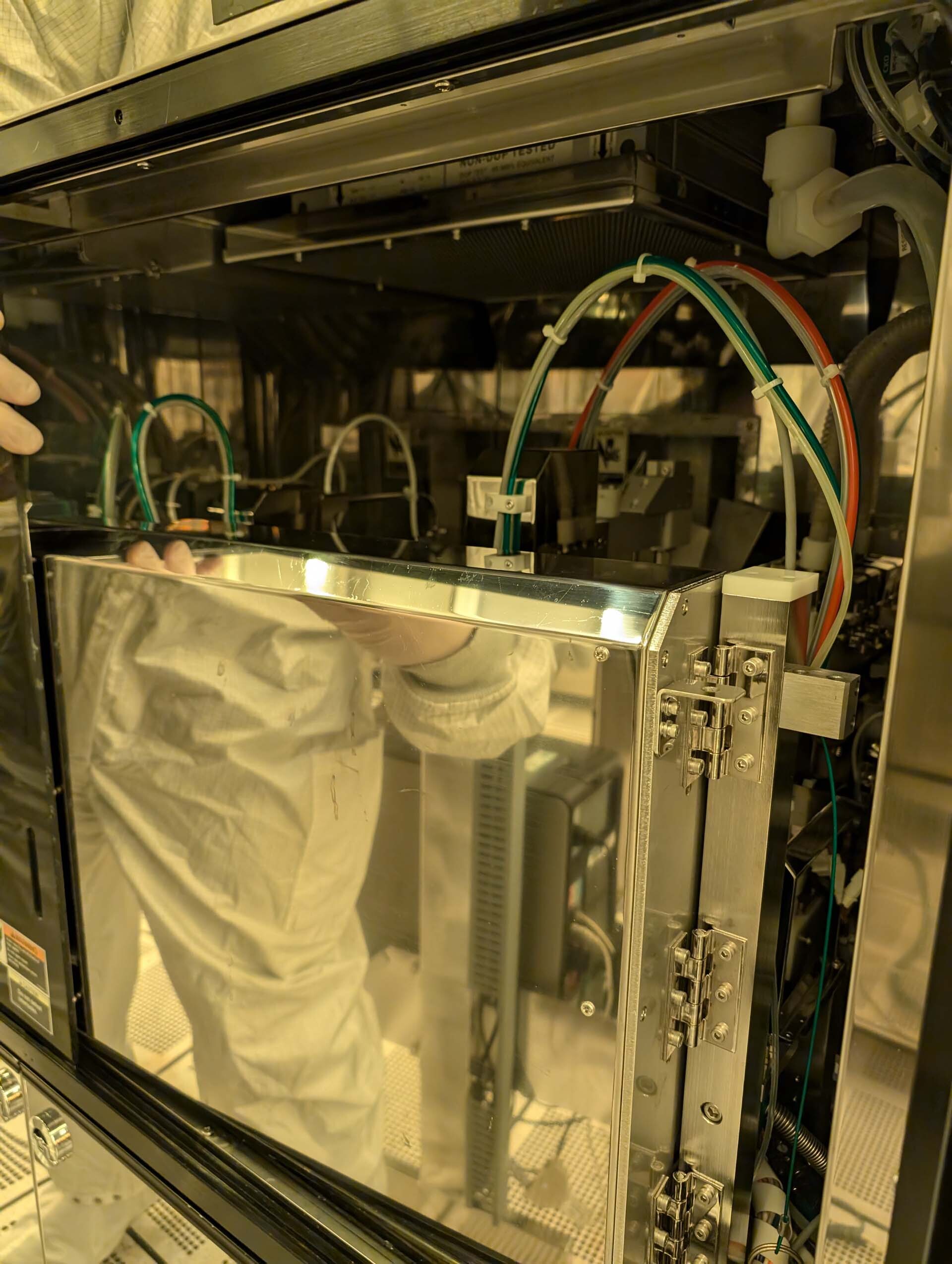
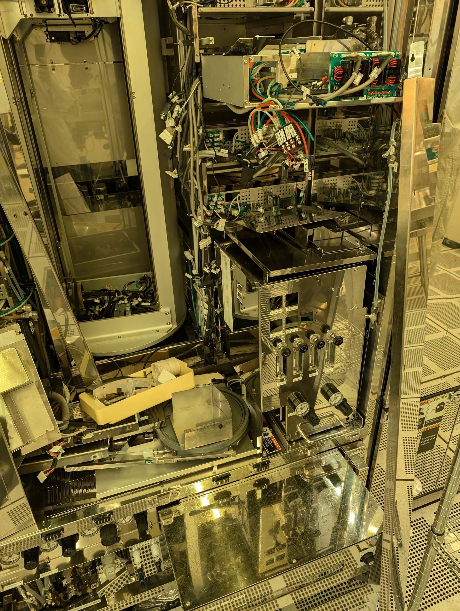
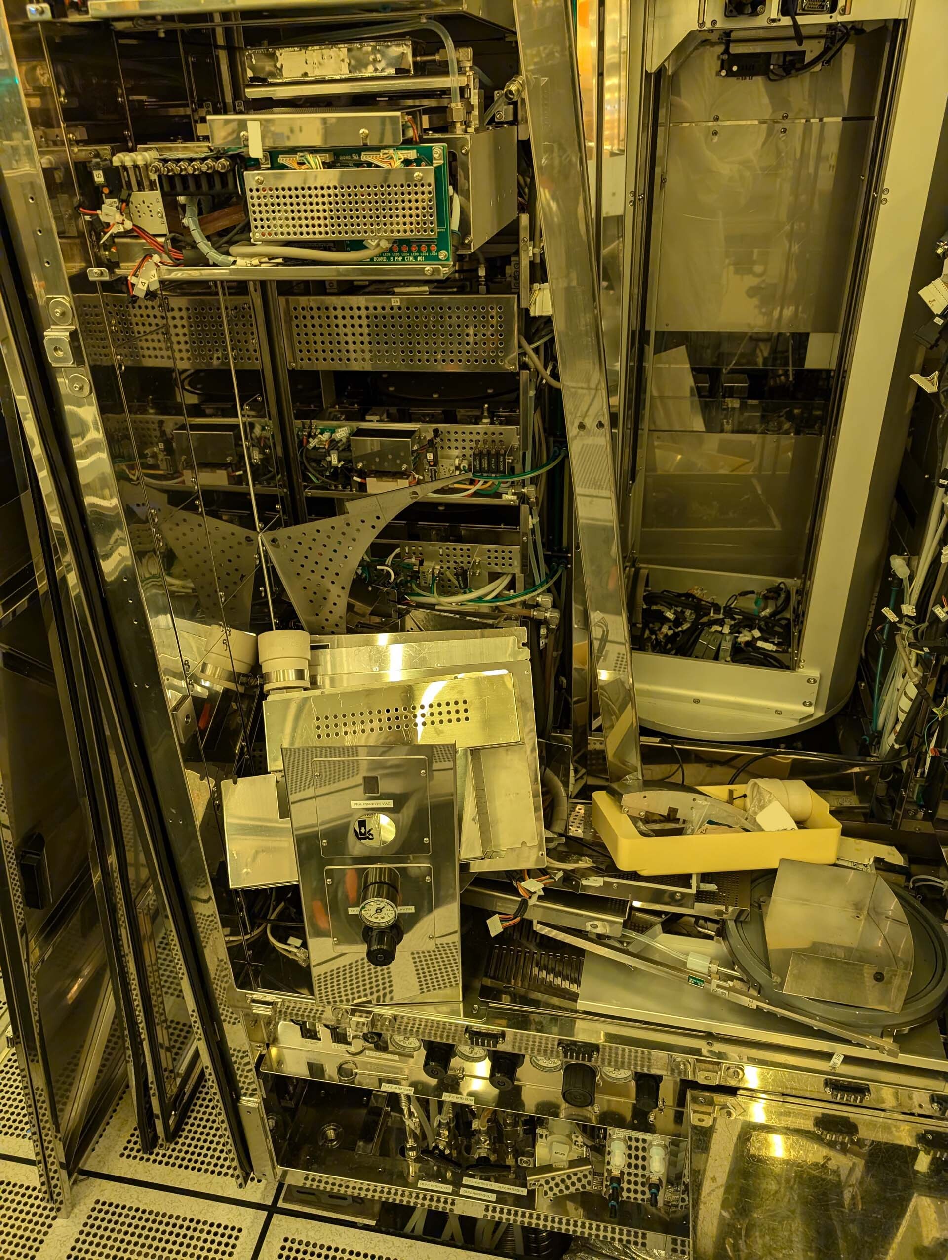
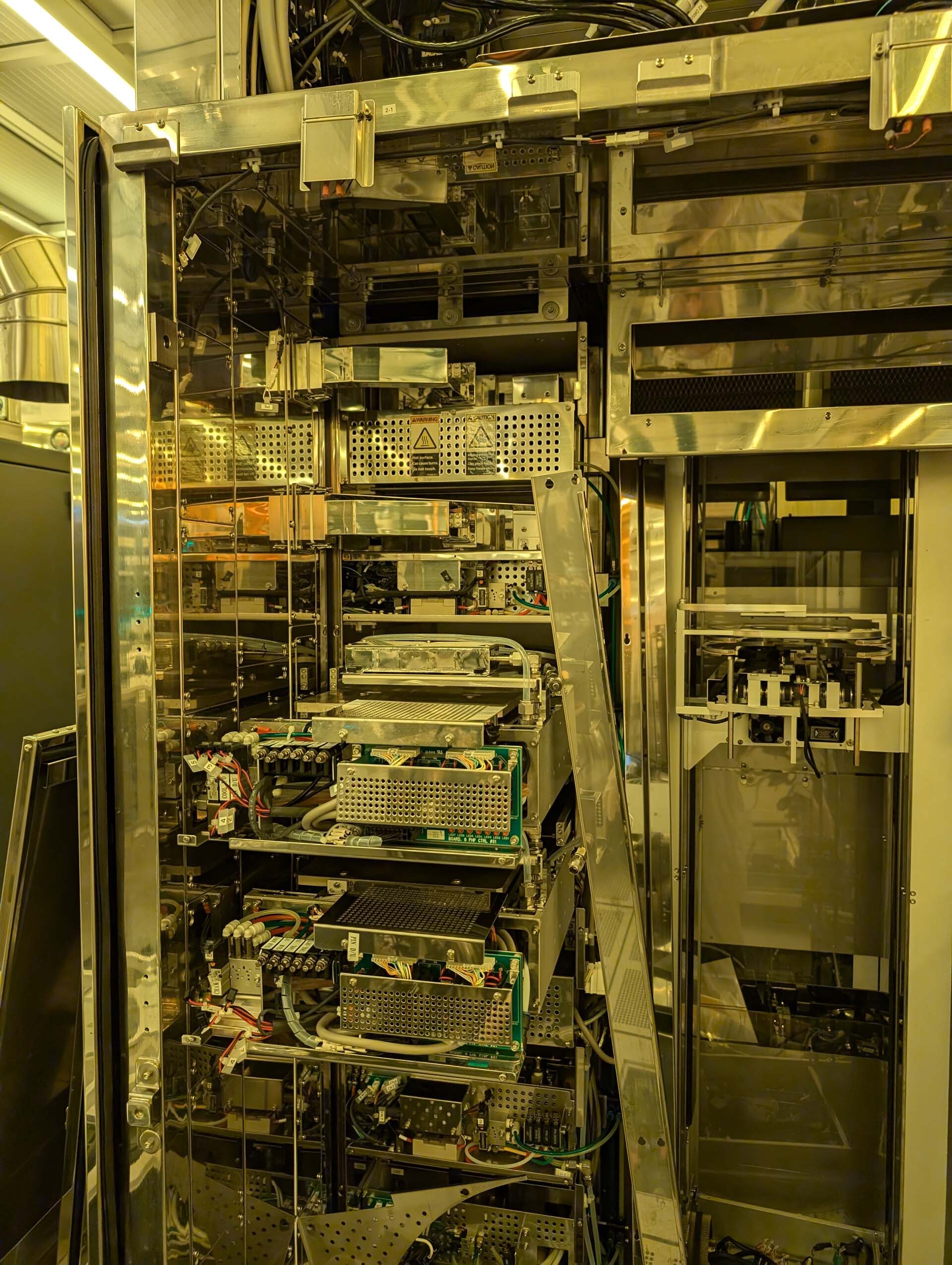
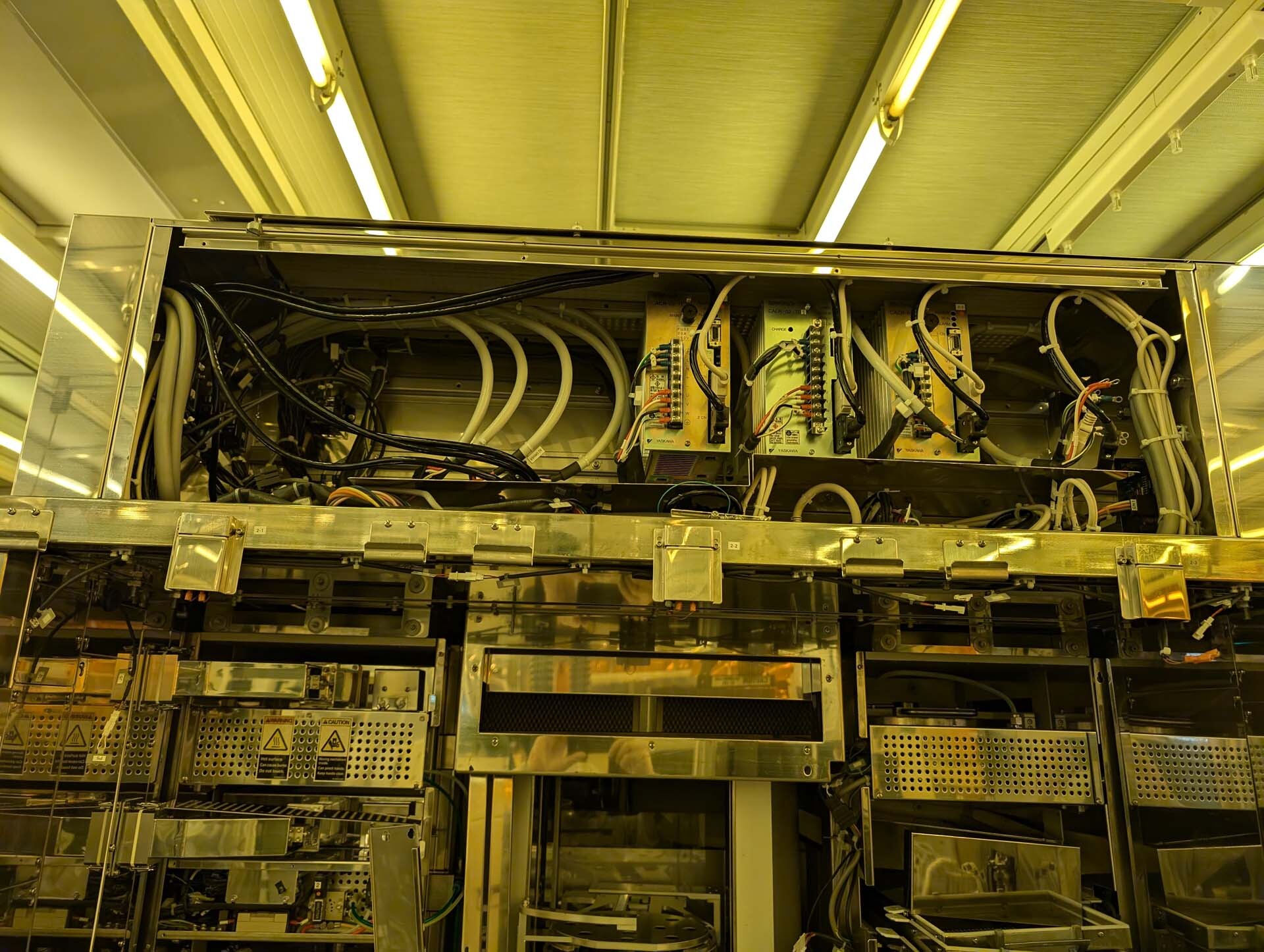
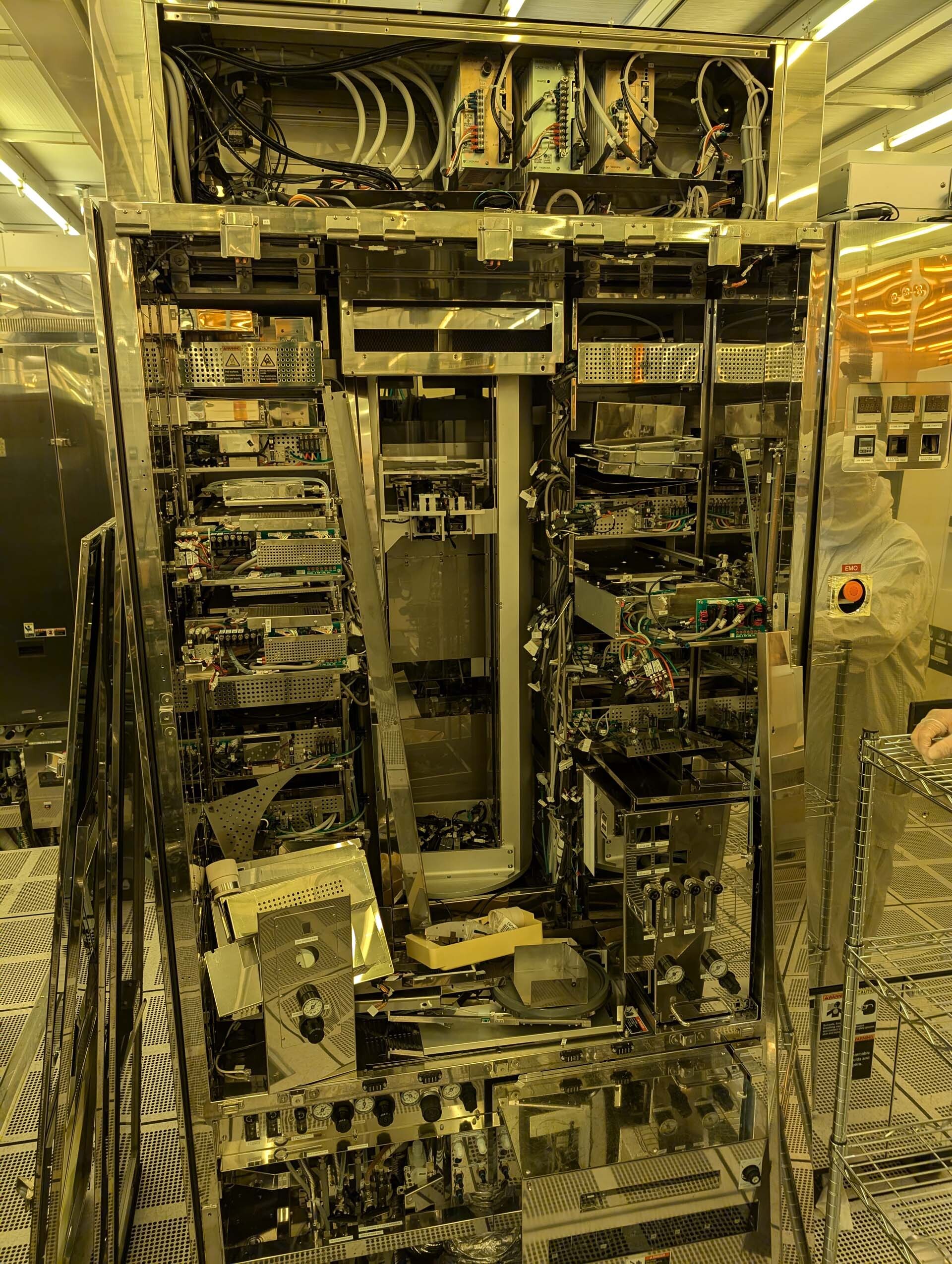
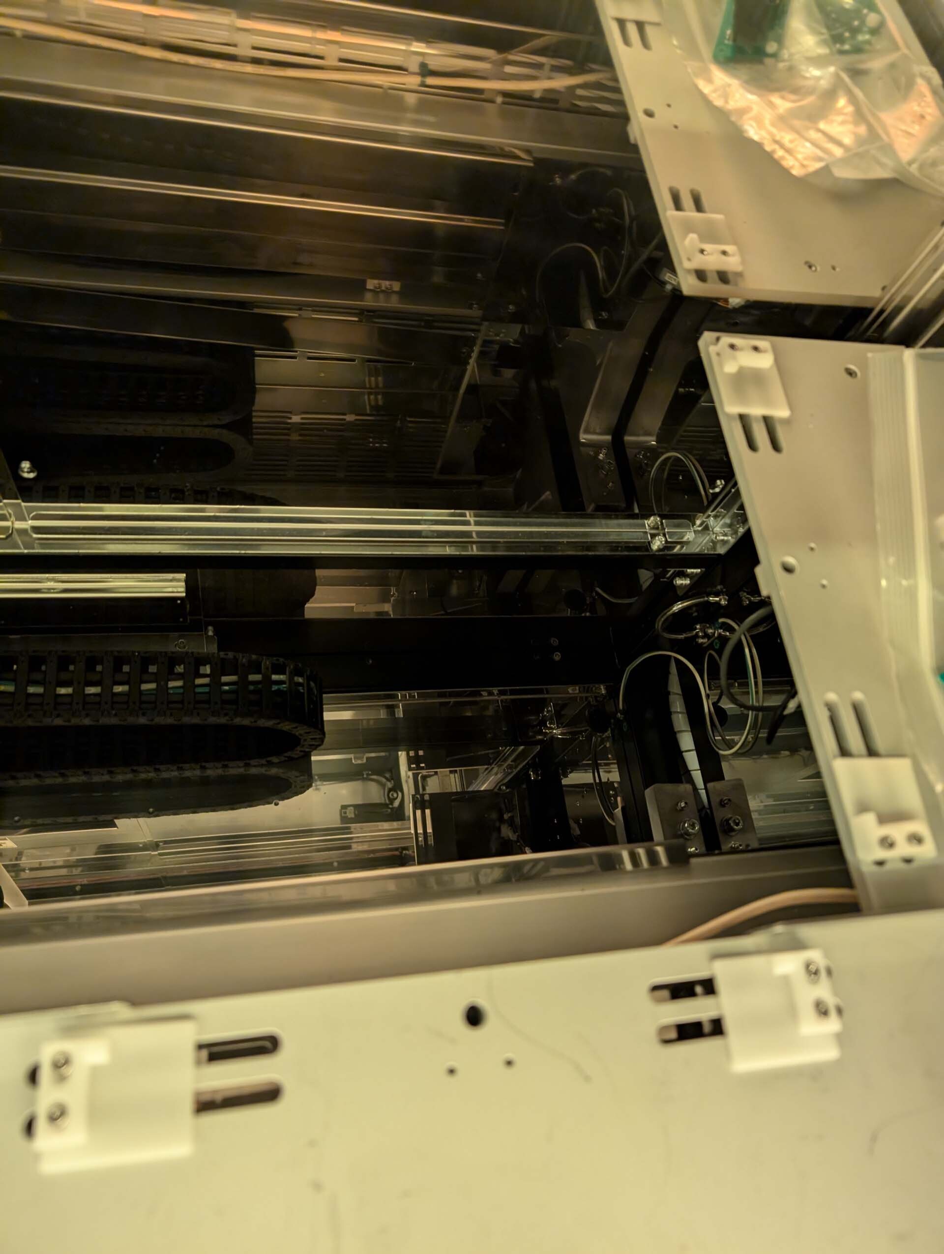
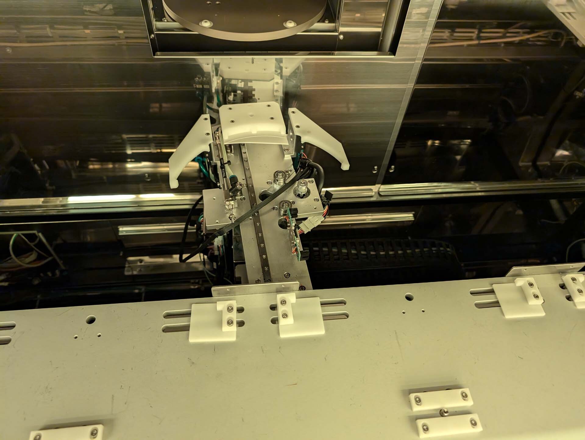
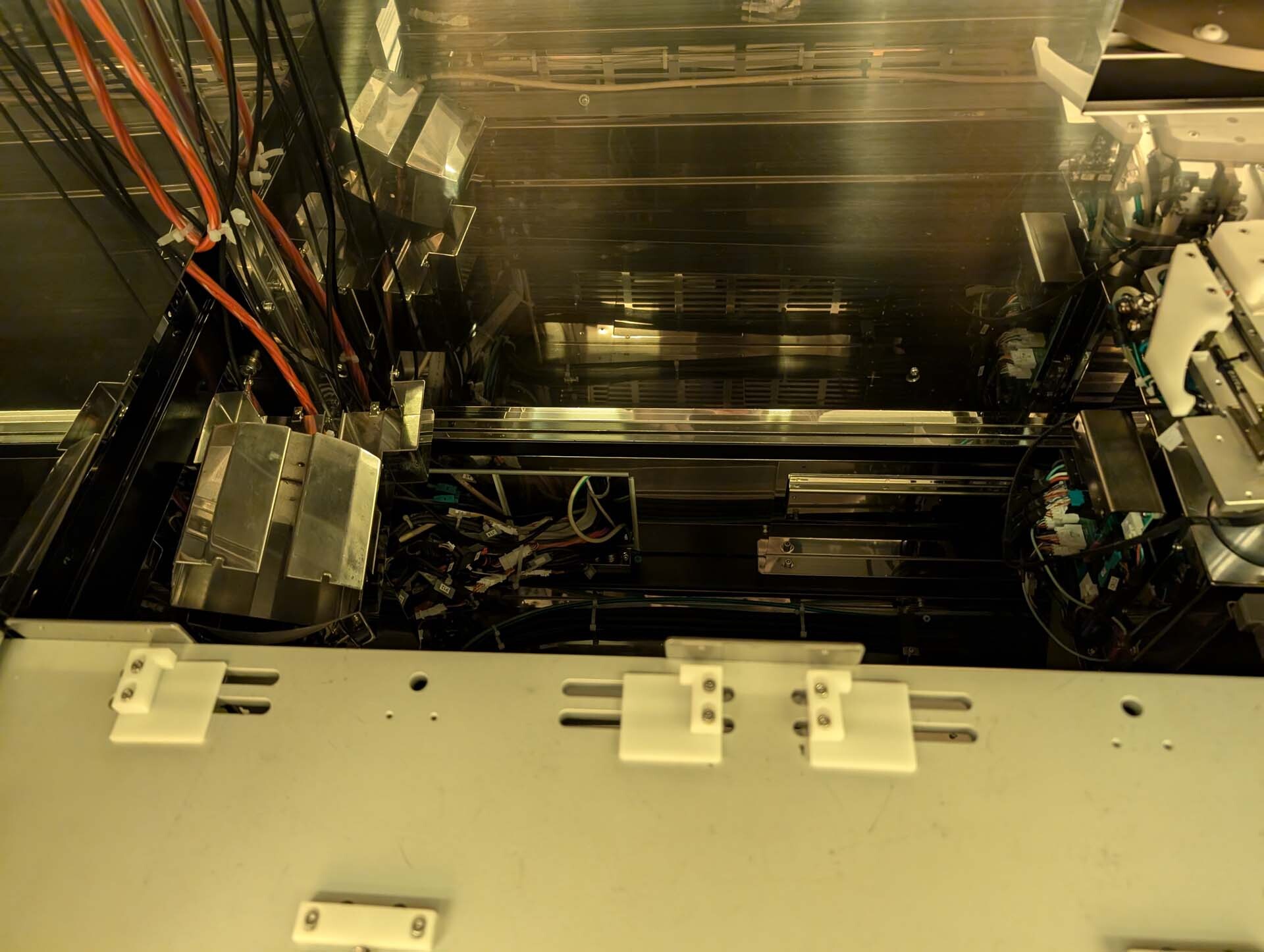
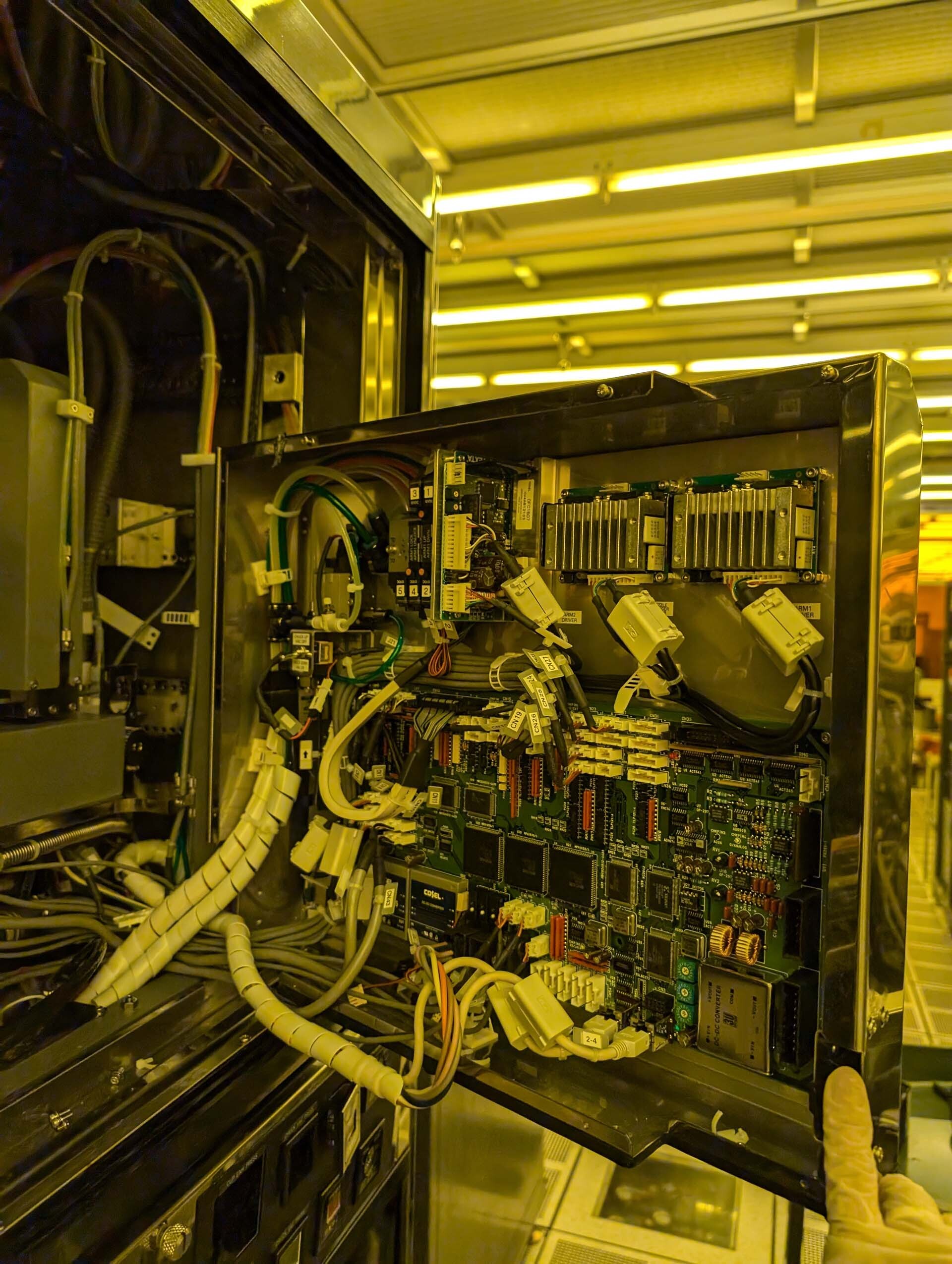
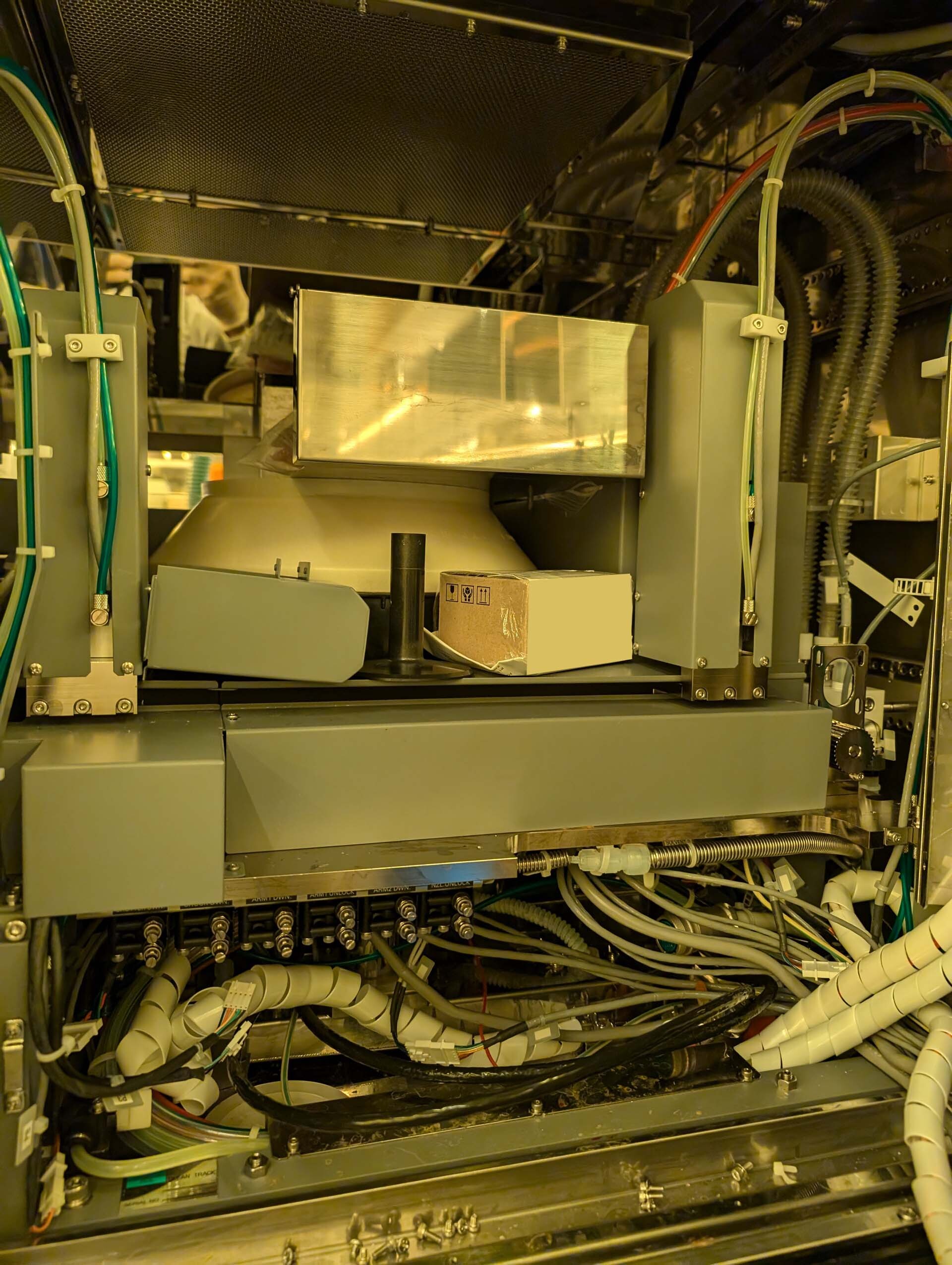
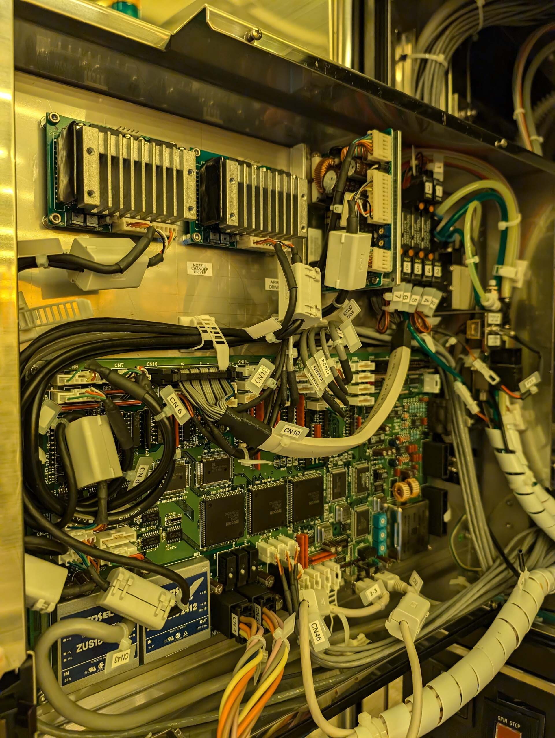
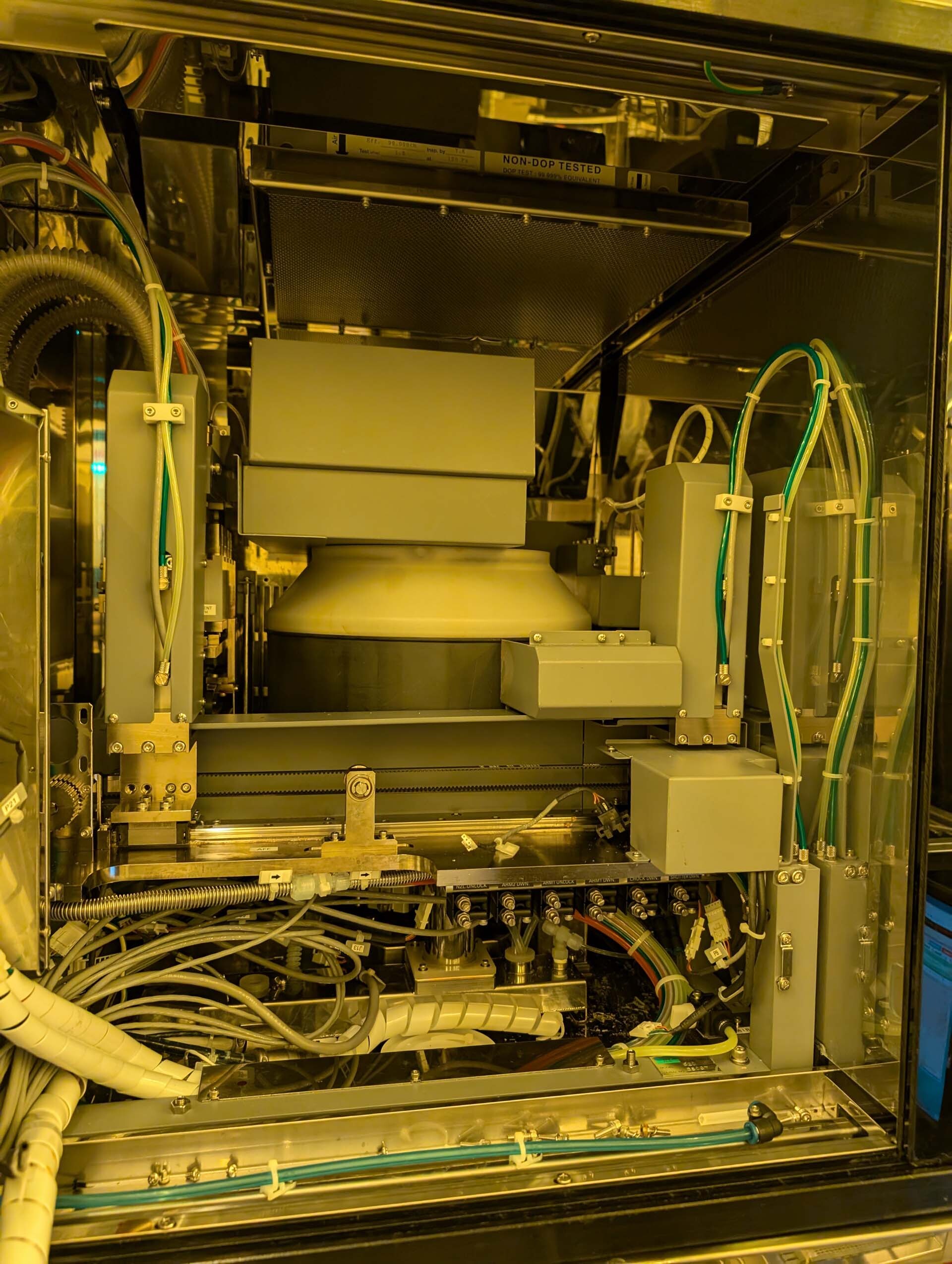
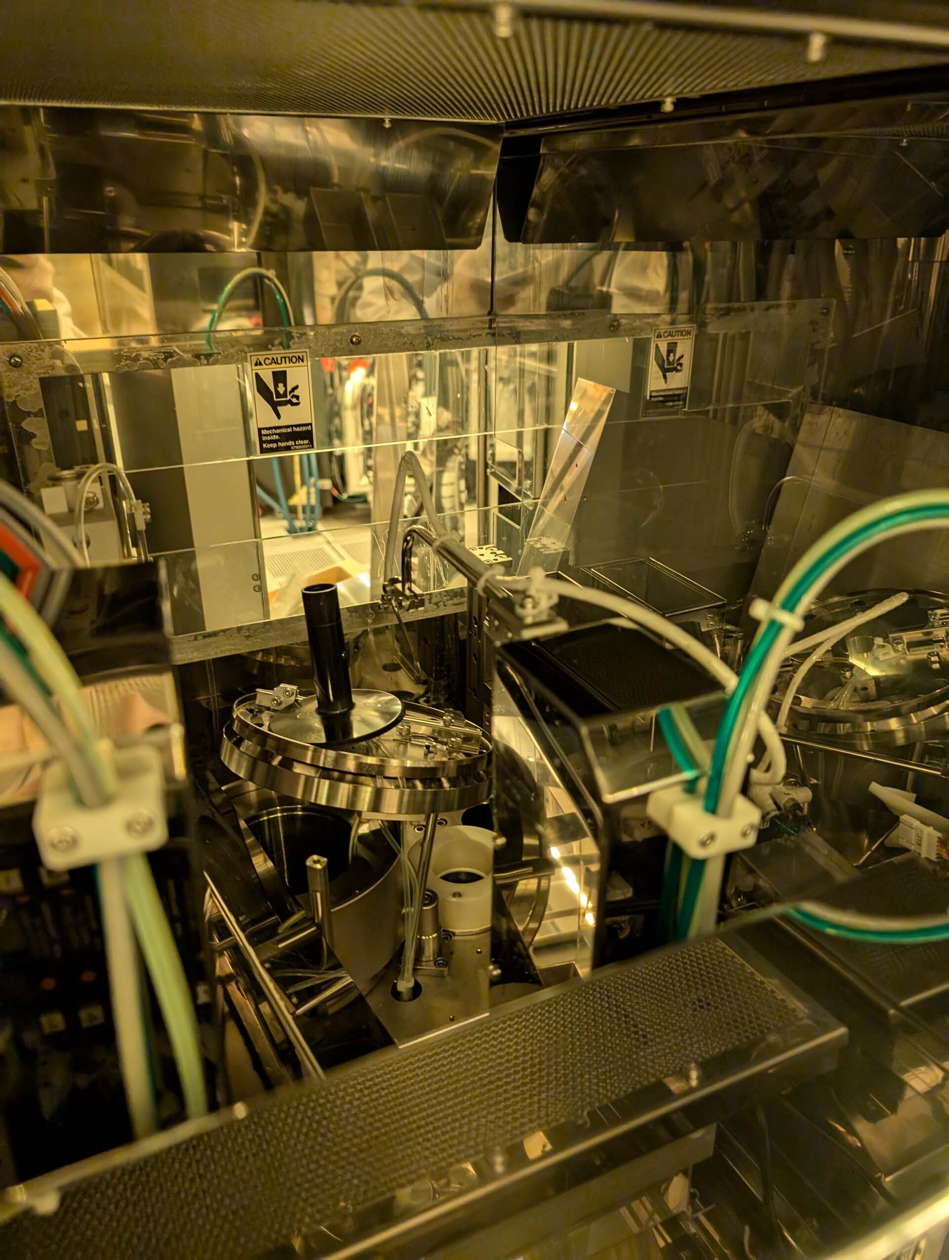
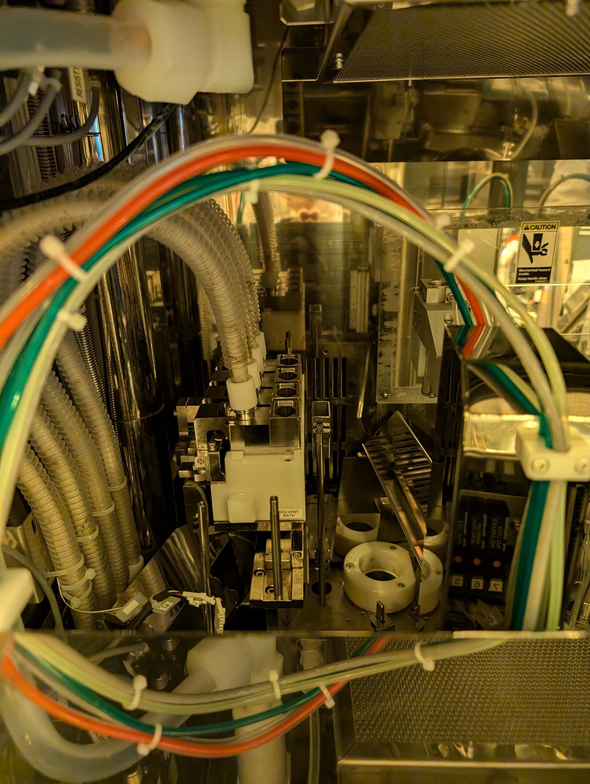
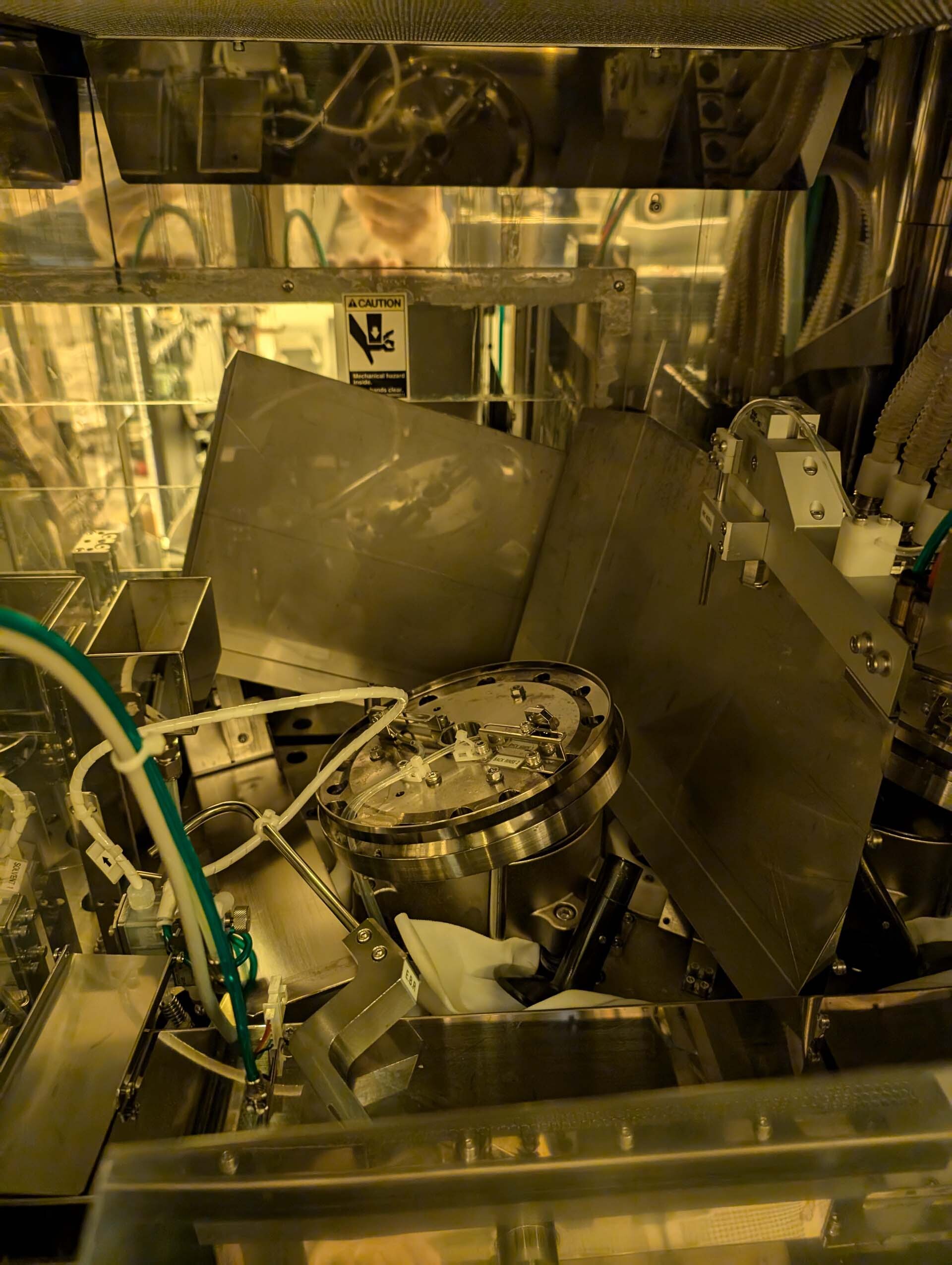
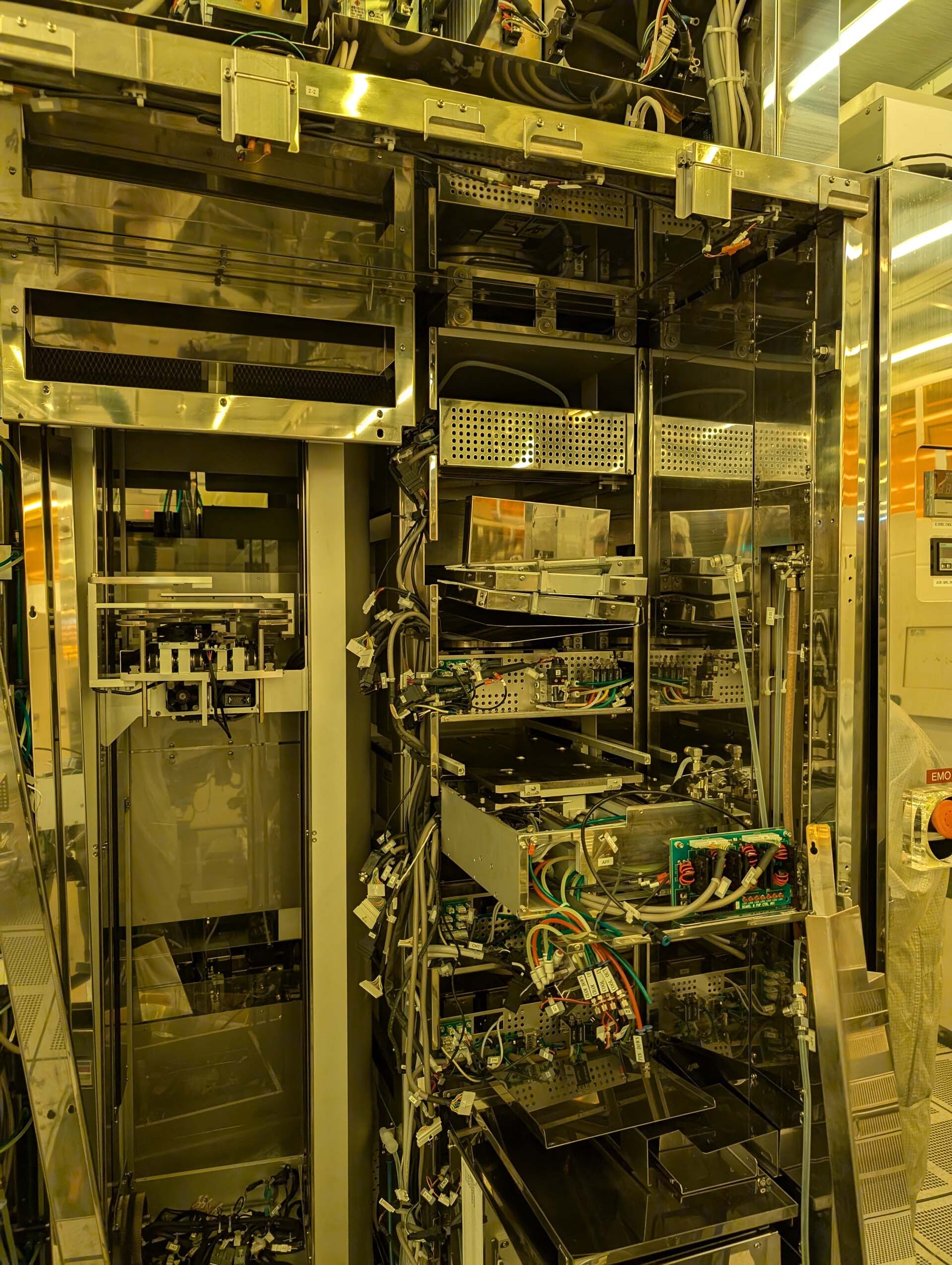
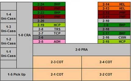
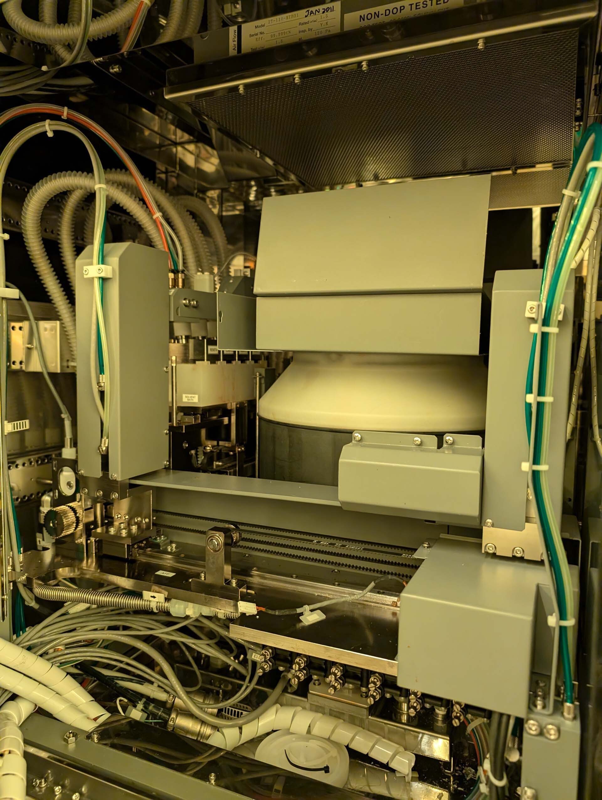
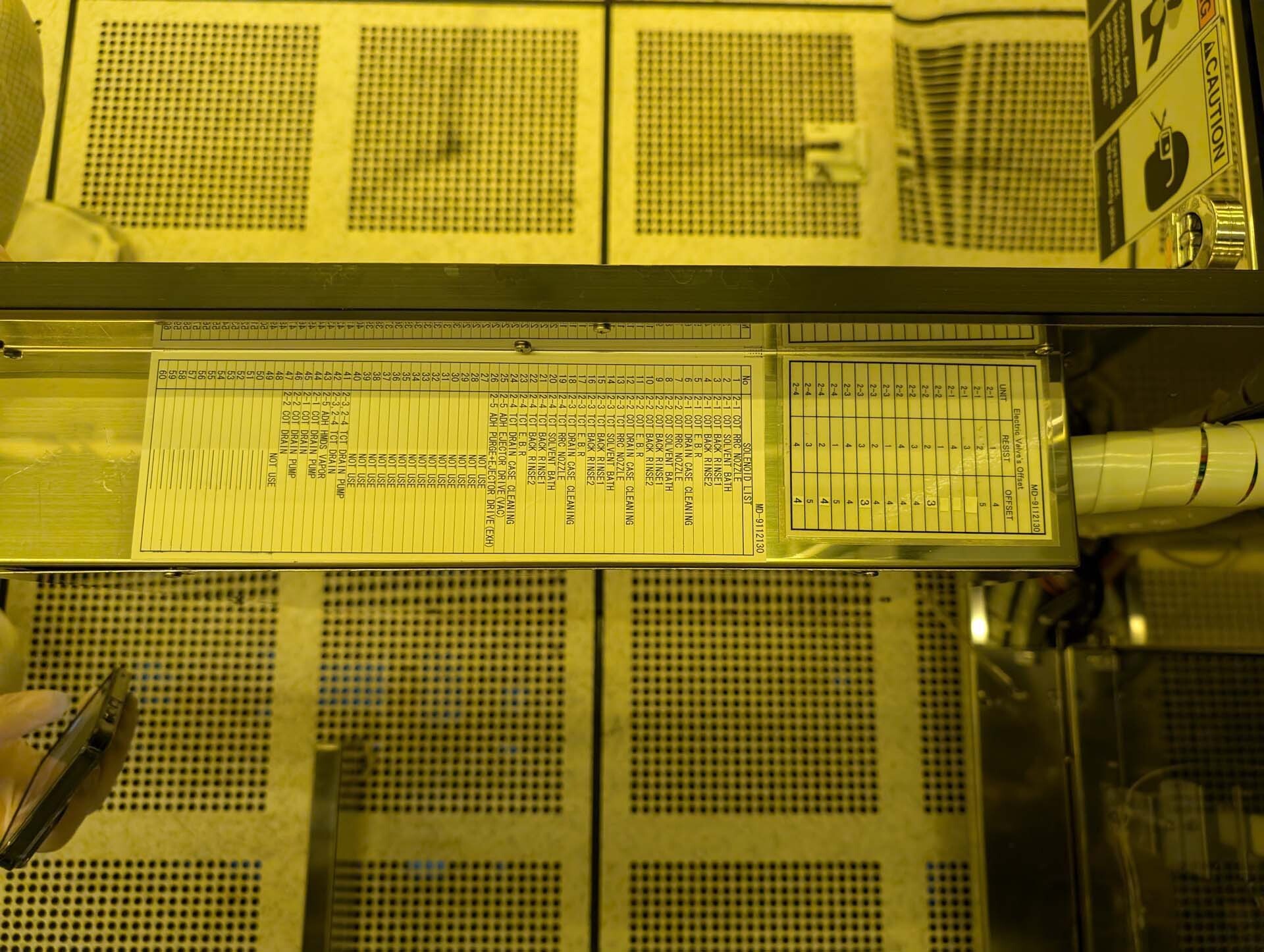
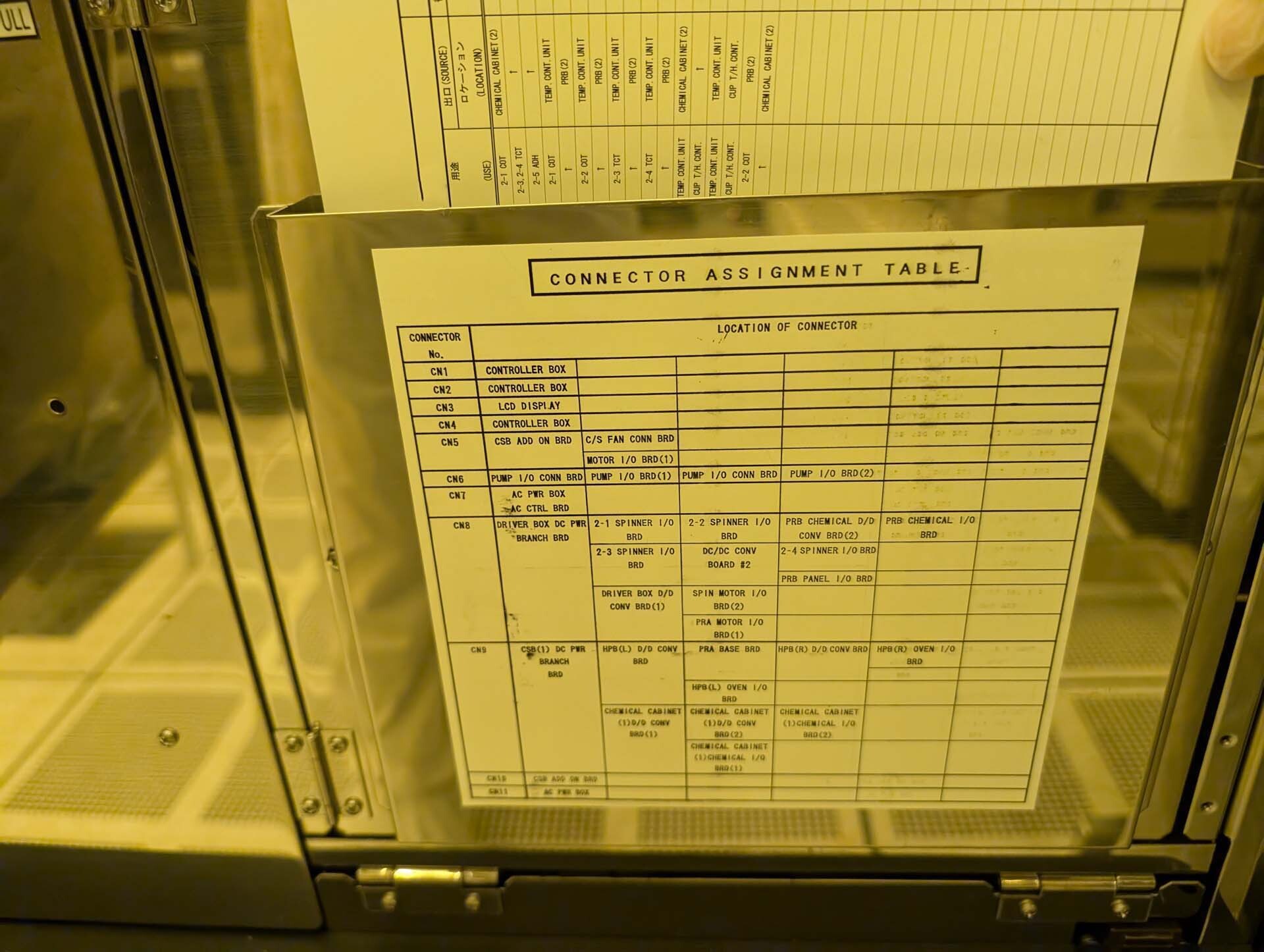
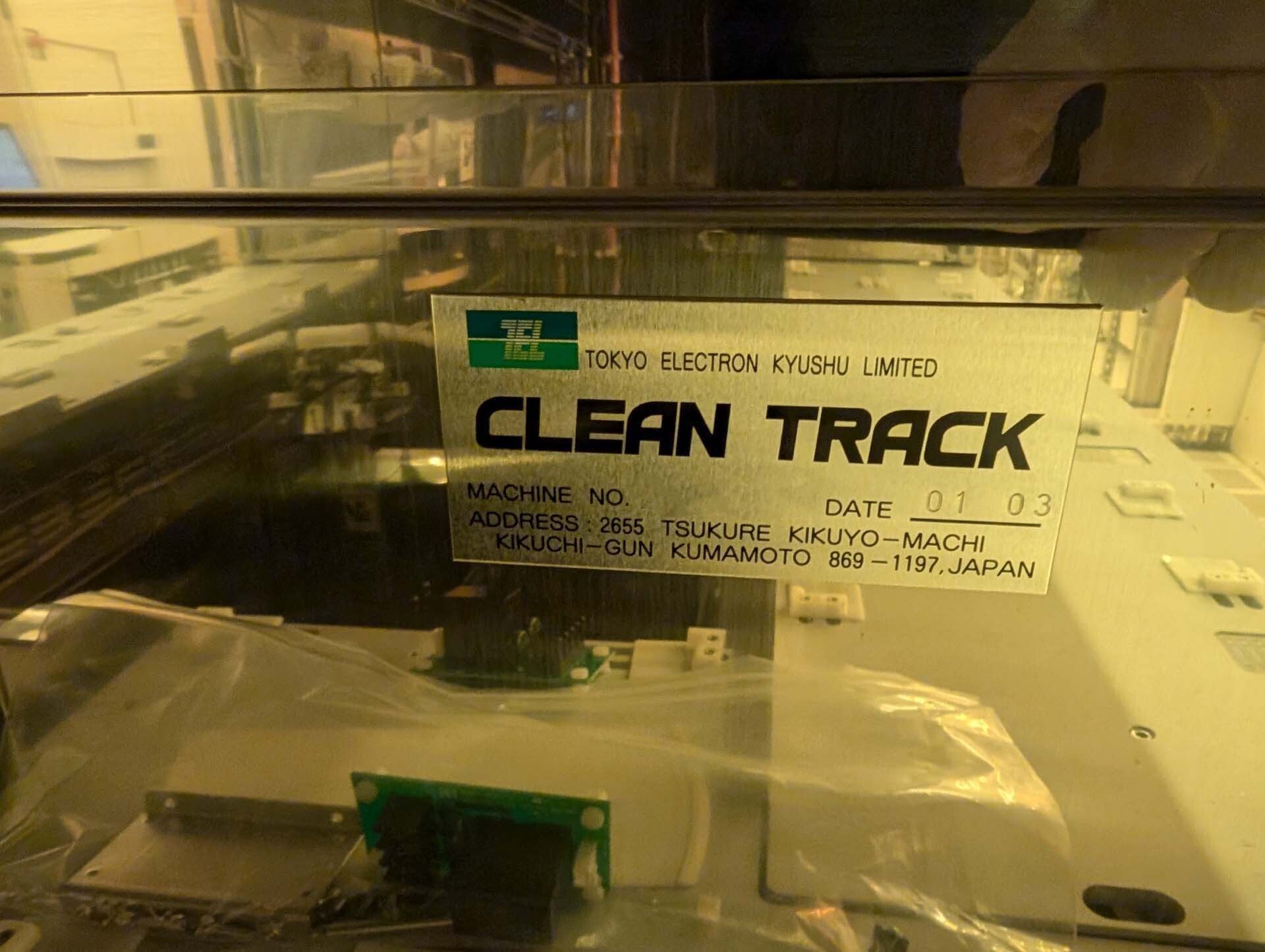
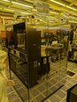
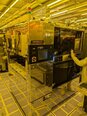
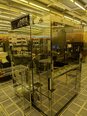
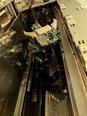
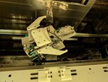
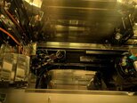
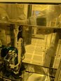
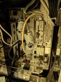
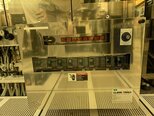
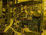
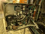
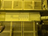
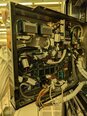
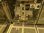
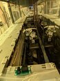
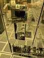
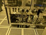
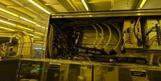
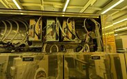
TEL / TOKYO ELECTRON ACT 8 is a high-performance photoresist equipment designed for use in advanced semiconductor fabrication processes. Photoresist systems are configured to control the exposed pattern of a photoresist film on a wafer. This type of process is necessary in order to achieve the extremely precise patterns and specific geometries required in modern, sophisticated chips. TEL ACT 8 system is composed of three main components: the Dispense Unit, the CD Measurement Machine and the Laser Direct Writer. The Dispense Tool enables the precise delivery of photoresist film materials onto the substrate. The CD Measurement Asset is designed to measure the critical dimensions of circuit patterns on the photoresist film for accuracy and precision. Finally, the Laser Direct Writer outputs a highly precise laser beam onto the photoresist that sharply delineates targeted circuit patterns. TOKYO ELECTRON ACT 8 model features performance-enhancing technologies, including a scanning electron microscope imaging equipment that facilitates rapid automated image processing and a high-power harmonic wave pulse generator for conformal writing of 3-dimensional photoresist patterns. The machine also has an optimized Beam Profile Stabilizer and a Next Generation Proximity Effect Correction Module. These features ensure highly precise photoresist patterns with margin-less integrity maintained by precision pattern compensation. The system is further able to measure the exposure dose of photoresistfilm to provide feedback on the exposure process. TOKYO ELECTRON ACT 8 unit is programmed with advanced control and monitoring algorithms, designed to provide total control over the exposure process. It has built-in database management capabilities, which allow the user to record parameters and results in real-time throughout the exposure process. The machine connects to the host computer via a local area network to provide communication with other equipment and personnel. ACT 8 accurately and precisely delivers film exposure patterns that enable high product yields in the fabrication process from photosensitive resist layers applied to wafers. Its combination of highly reliable film delivery, precise pattern recognition and control, and efficient image analysis combined with advanced control and database capabilities make it an essential tool for modern semiconductor product manufacturing.
There are no reviews yet