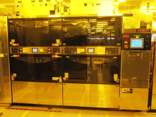
Used TEL / TOKYO ELECTRON Clean Track ACT 8 #9190707 for sale
It looks like this item has already been sold. Check similar products below or contact us and our experienced team will find it for you.
Tap to zoom


Sold
ID: 9190707
Wafer Size: 8"
Vintage: 2000
Resist coater / Developer, 8"
Multi block
Wafer type: Notch
In-line with stepper type: NIKON B12
Wafer flow direction: Right to left
Spinner unit configuration: 2C
Function of coater heads: (4) Nozzles / Coater
With individual pump per nozzle / Prewet nozzle
Main body frames: (3) Blocks
Indexer
Coater / Developer
Interface
SMIF: (3) Indexers
Robot arm: Ceramic / Aluminium
LHP: 250 deg (+/- 2deg)
PCHP: 150 deg (+/- 2deg)
CPL: 22 deg (+/- 2deg)
Cooling plate temperature control system: PID Controller
Spin developer head: 4D
Functions for developer coater heads:
(2) Developer lines with H Nozzle / DIW Center rinsing
Developer dispense: N2 Pressure
DIW Rinse with flow meter:
Top-side
Back-side
Programmable exhaust damper (Screen std)
Filter for developer and DIW (Pall DFA1FTS 64M, 0.1um):
CHUV2LOP1
UPE Filter: 100 nm
Developer temperature control system: ETU Controller
Chemical cabinet
Drain pans
With leak sensors (Main body and DD cabinets)
Double containment for chemical lines: DD Cabinet to main body (EBR / Cup rinse)
TEL Tower lamp
Power requirements: 220 V, 3 Phase, 4 Wire, 50-60 Hz
2000 vintage.
TEL (TOKYO ELECTRON) TEL / TOKYO ELECTRON Clean Track ACT 8 is an advanced photoresist equipment designed for precise, high accuracy, nano-patterning with superior performance to traditional lithographic techniques. The photoresist system provides a streamlined design and operation platform, which ensures the most consistent results in the shortest amount of time. The unit works by first exposing the substrate material to light (using an exposure machine) and then applying a photoresist onto the substrate. The photoresist acts as a masking layer, blocking some of the light from reaching the substrate material in areas on which the pattern is desired. The pattern is achieved by controlling the exposure time, intensity, and angle of the light source, as well as the composition of the photoresist. TEL Clean Track ACT 8 is designed with a robust set of features for operation, including an auto-focus tool to ensure accurate lithography requirements every time, an enclosed chamber with a pneumatic door, programmable adjustments and host of other features. The advanced features of this asset allow for patterning in a range of layers/layers, from the micron to the sub-micron range, with a minimum feature size of 10nm being achievable. This model is ideal for chip manufacturing, targetting semiconductor devices, microelectromechanical systems (MEMs), display technology, etc. The photoresist equipment comes with two main advantages. The first is a reduction in cost as only a single photoresist system needs to be used instead of multiple lithography modules. The second is an improved throughput as patterns can be drawn quickly without any manual interference by the operator. In addition to this, the unit can be optimized for the specific application requirements in order to produce more precise results in a shorter period of time. Examples of features which can be adjusted include the chemical composition of the photoresist, the layer thickness of the substrate material, and the pattern shrink coefficient. TOKYO ELECTRON Clean Track ACT 8 photoresist machine provides an ideal platform for data-driven development and patterning of nano-scale electronic devices. The tool leads to improved results with a shorter turn-around time, which yields both cost efficiencies and improved technology processes. It is the perfect solution for customers searching for a reliable and cost-effective platform to develop advanced, hi-tech applications.
There are no reviews yet