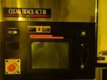
Used TEL / TOKYO ELECTRON Clean Track ACT 8 #9235975 for sale
URL successfully copied!
Tap to zoom
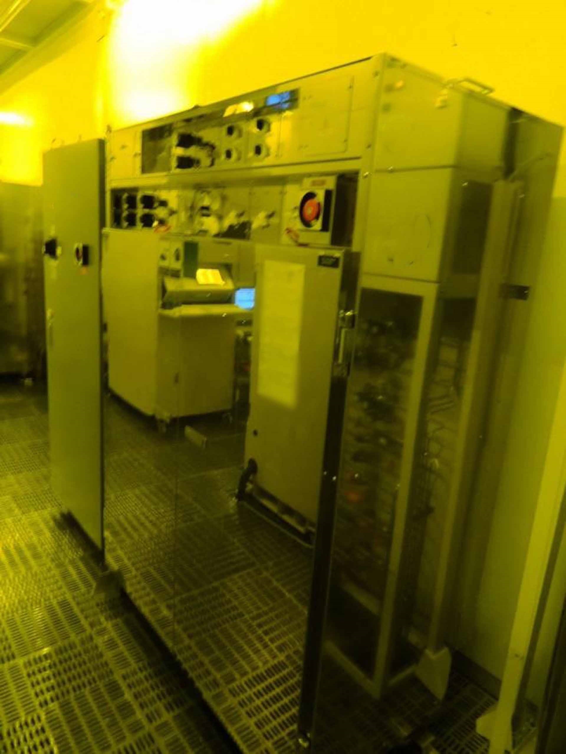

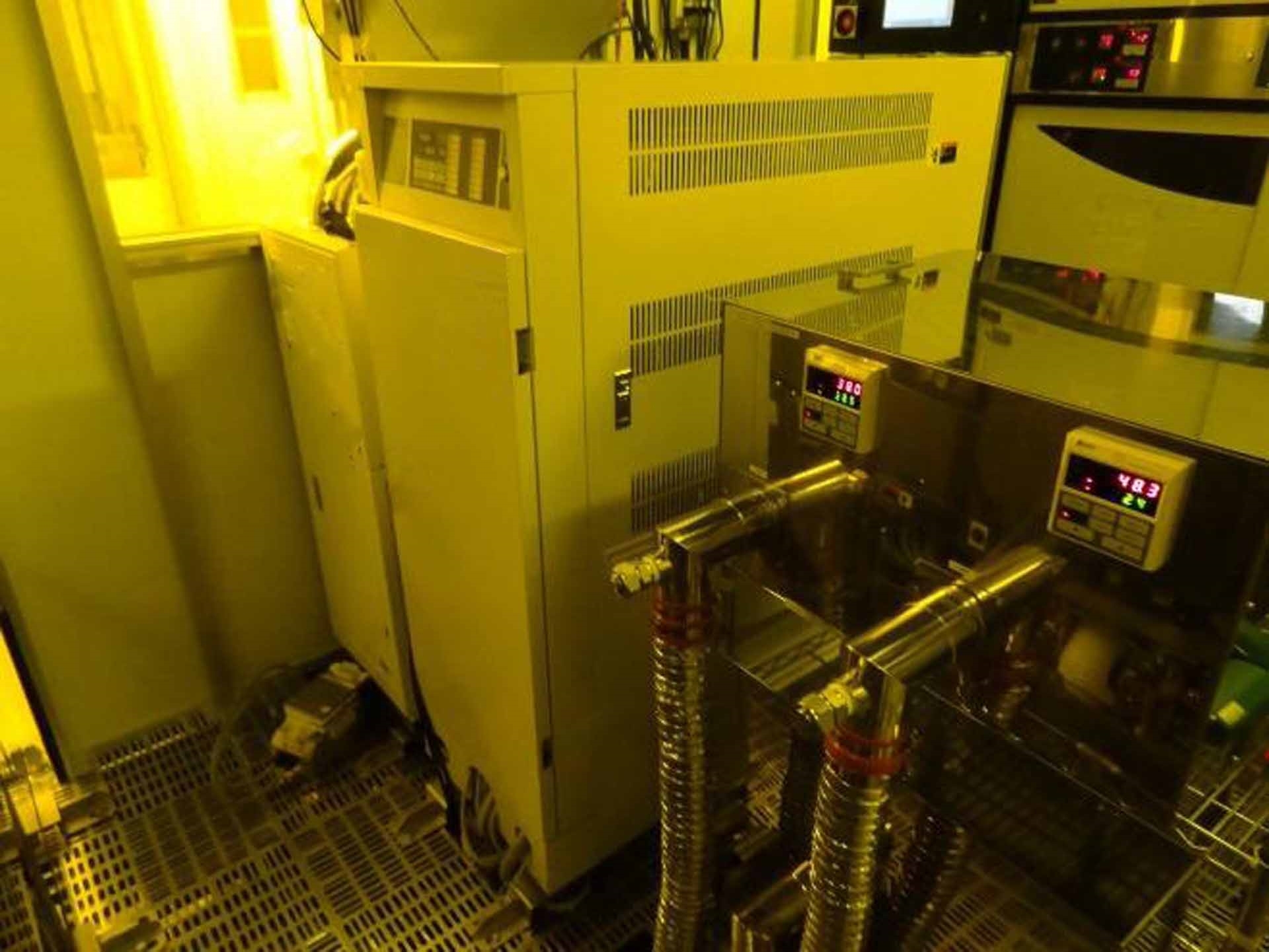

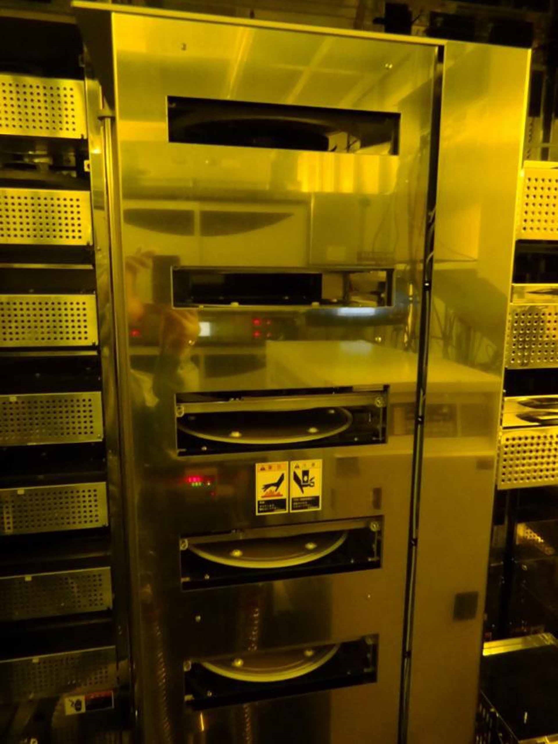

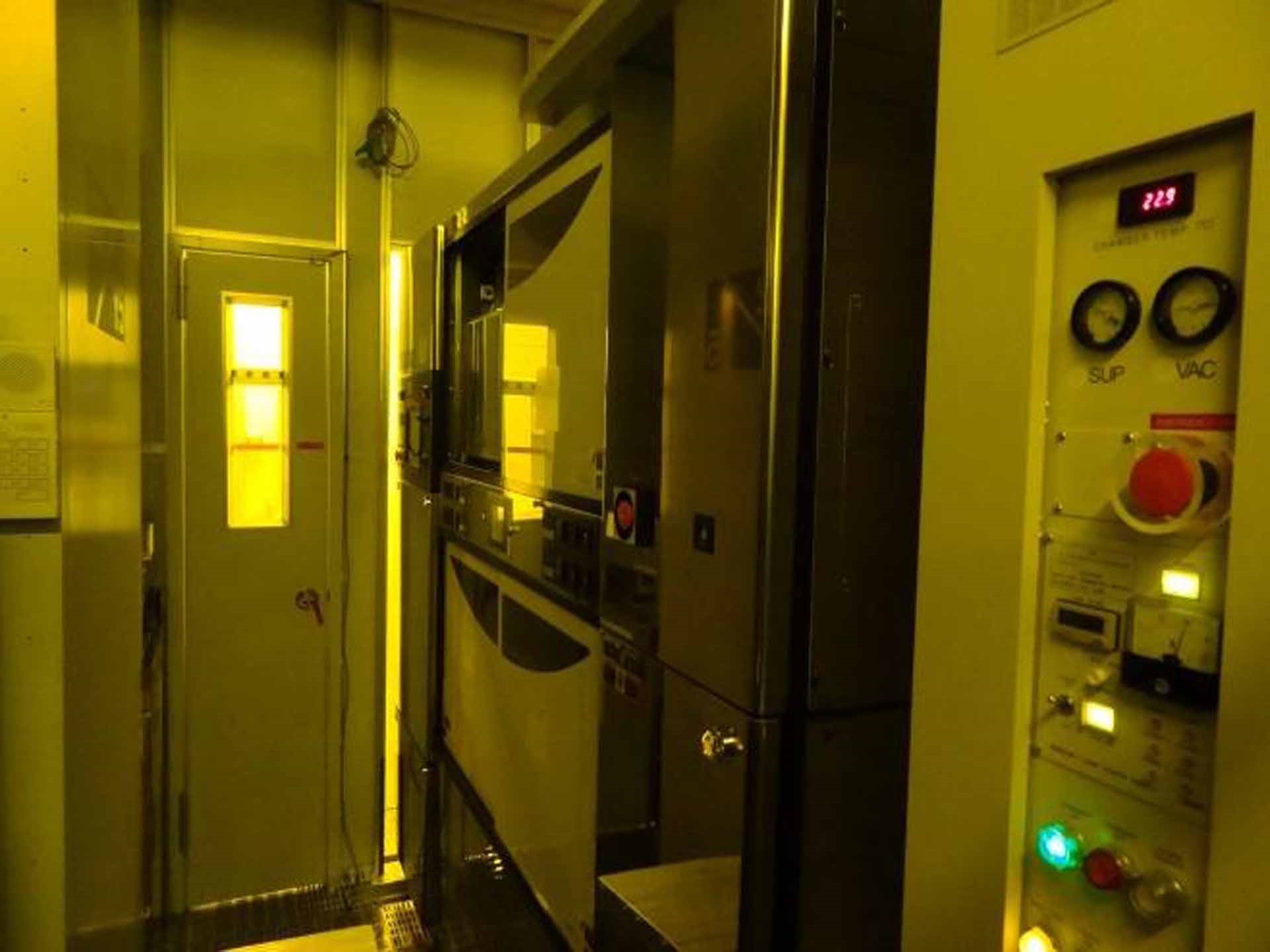

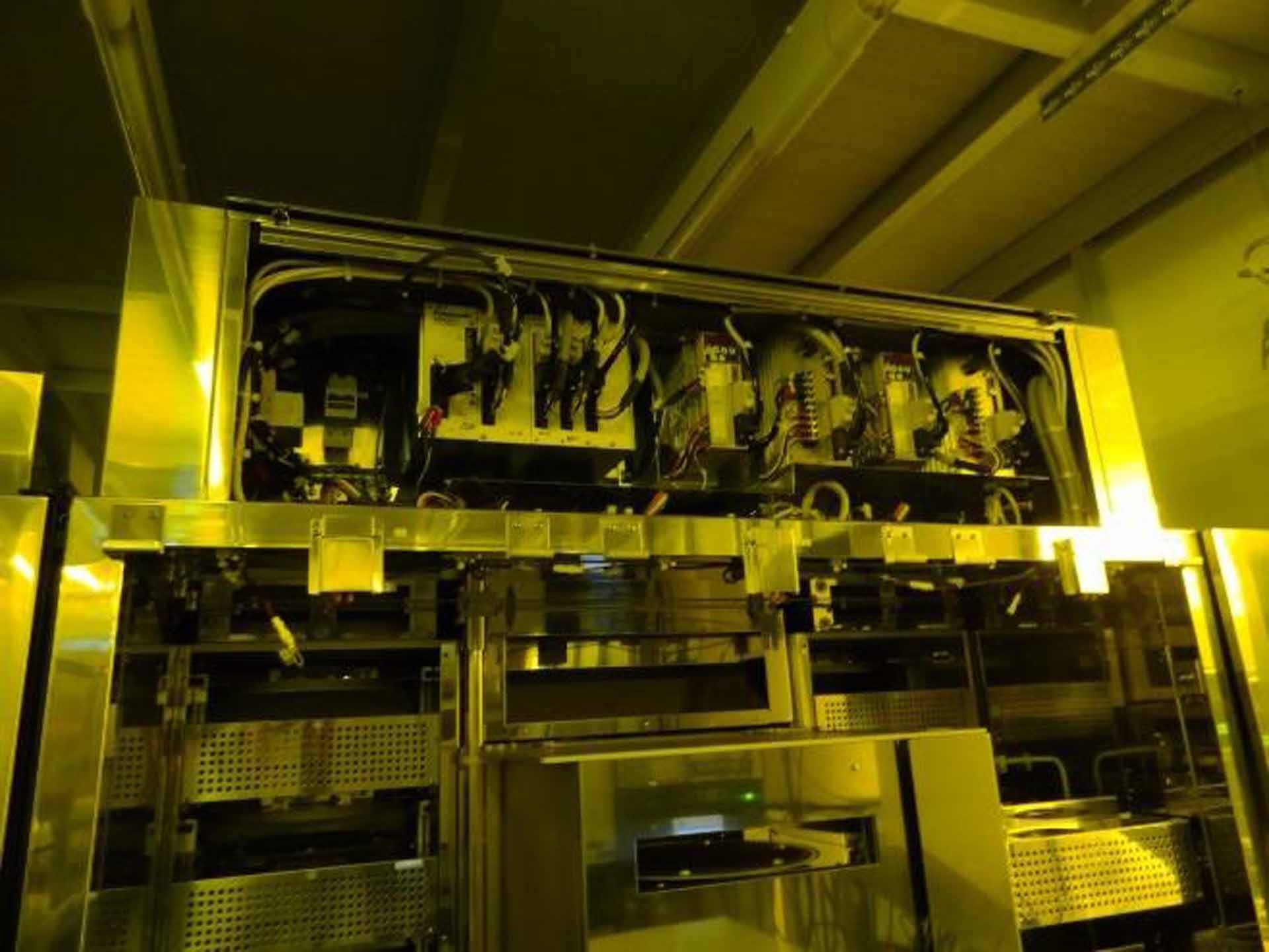



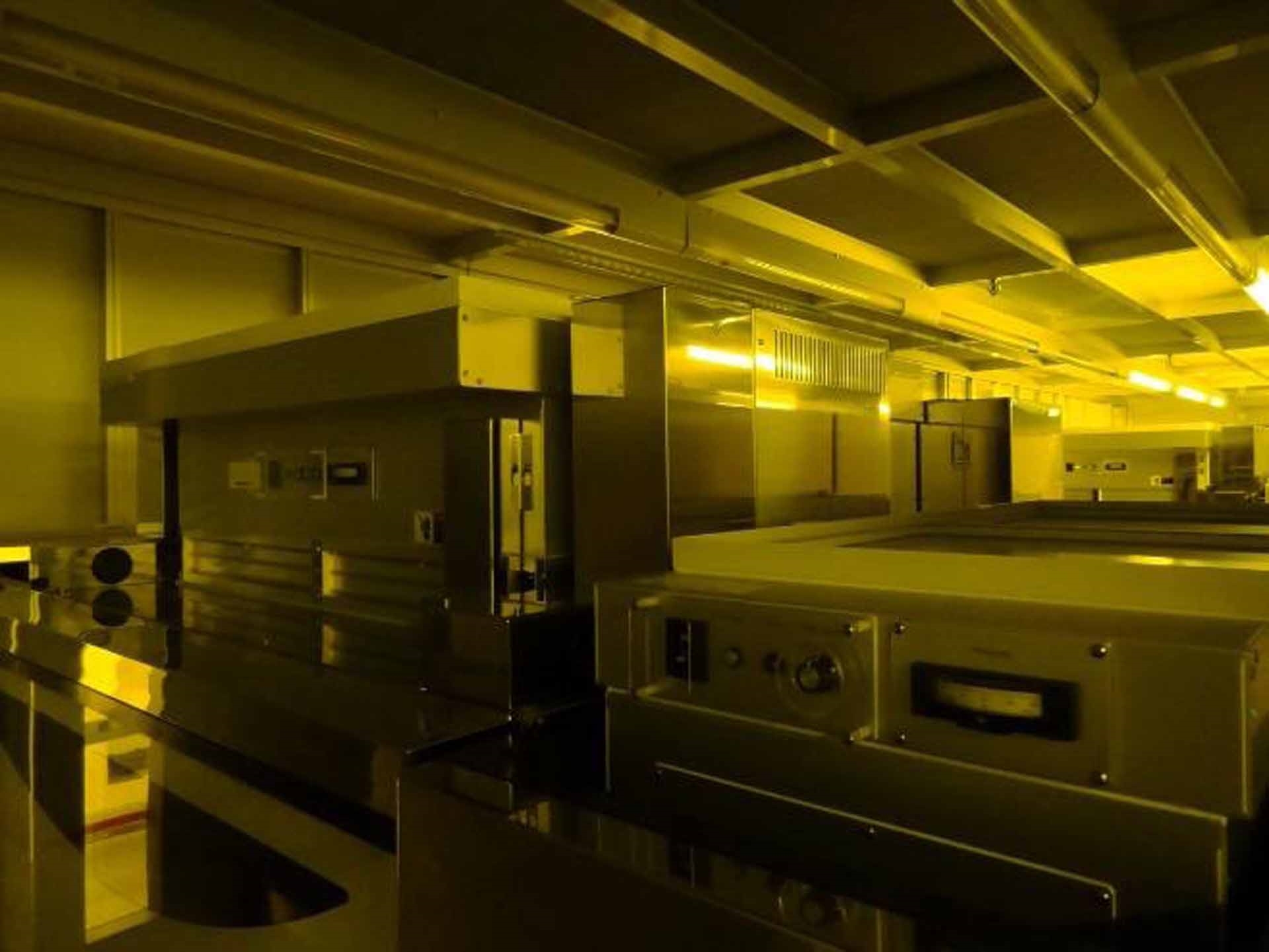


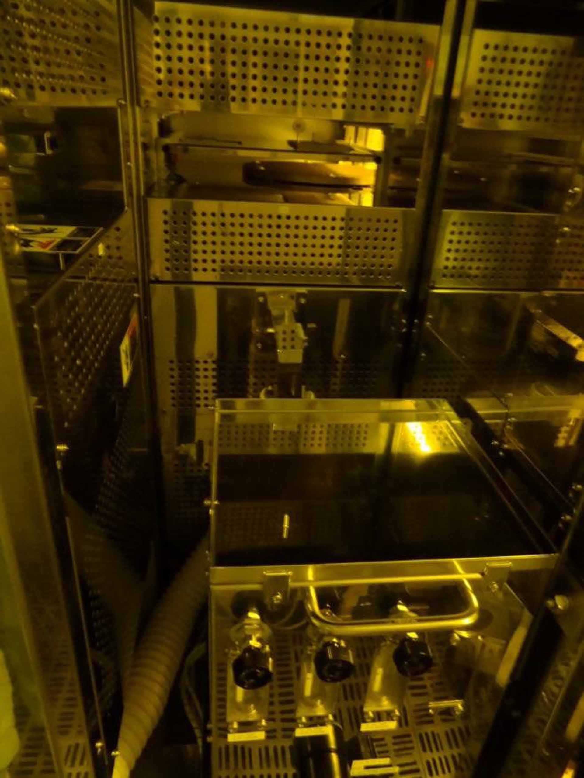

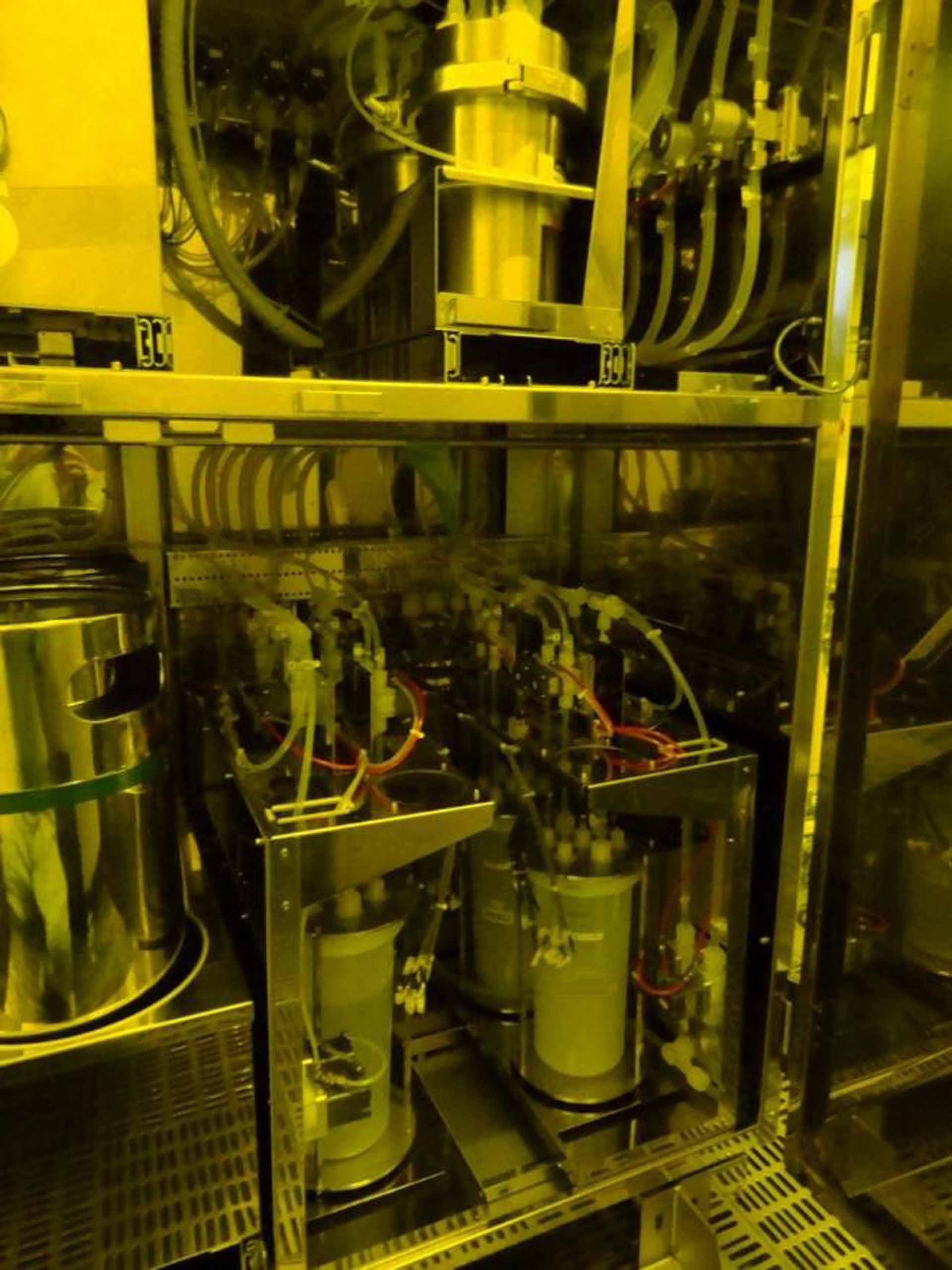

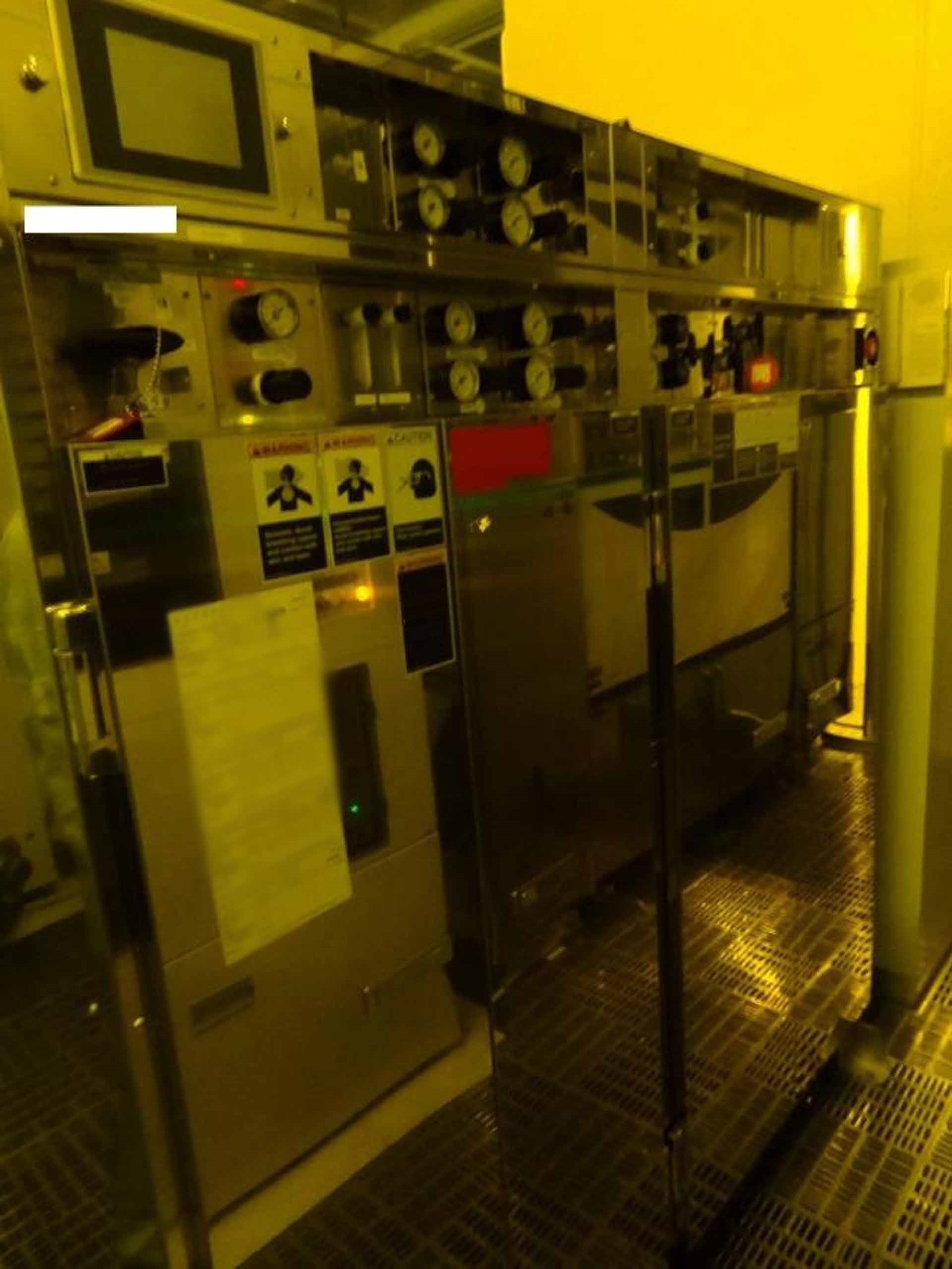

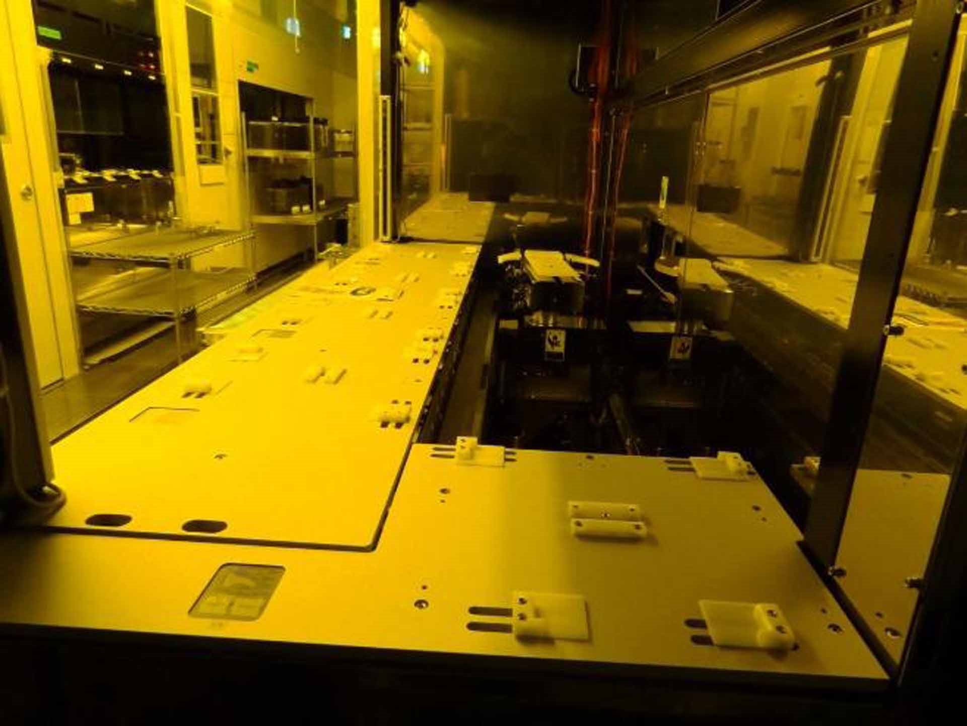


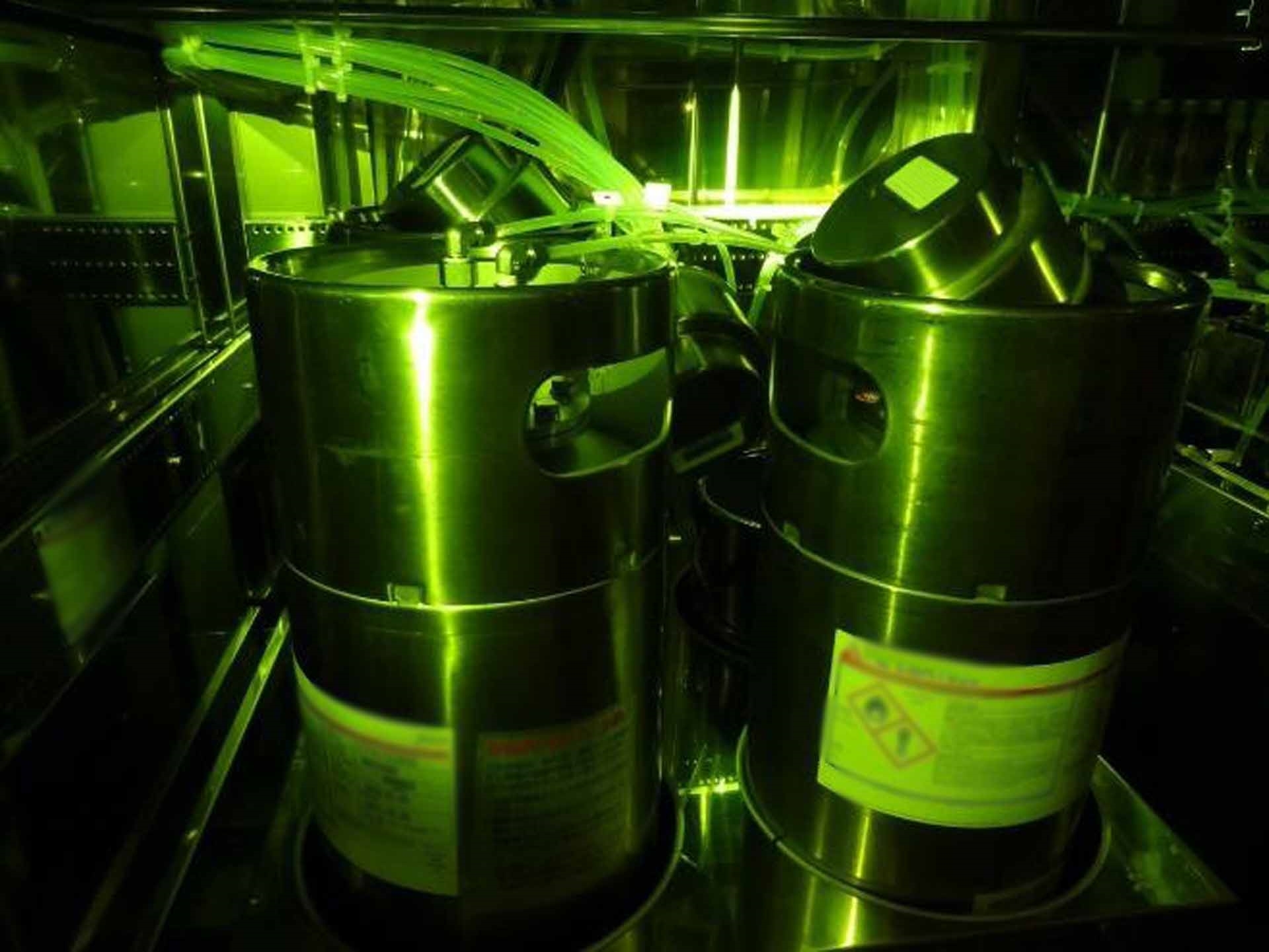



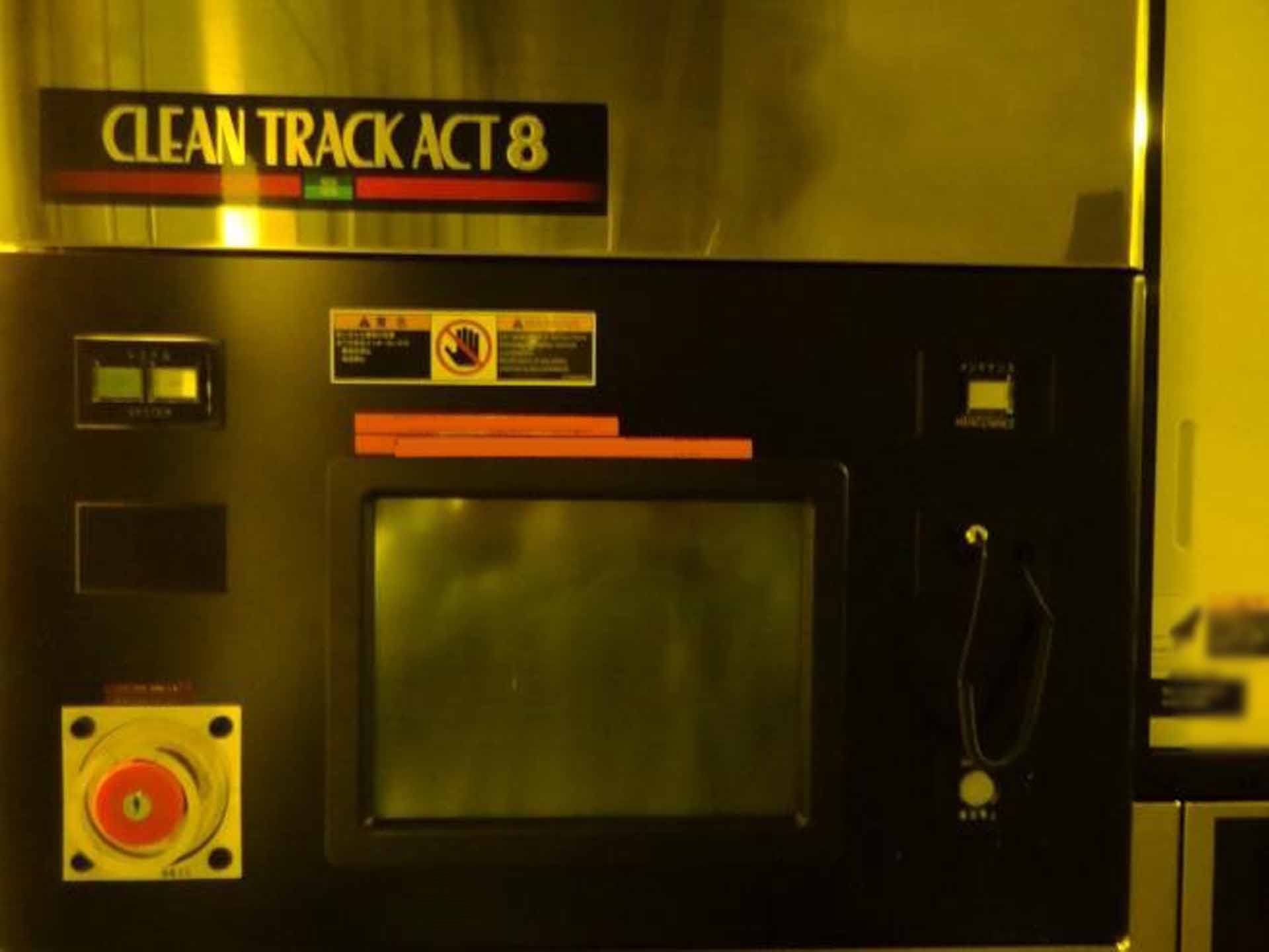

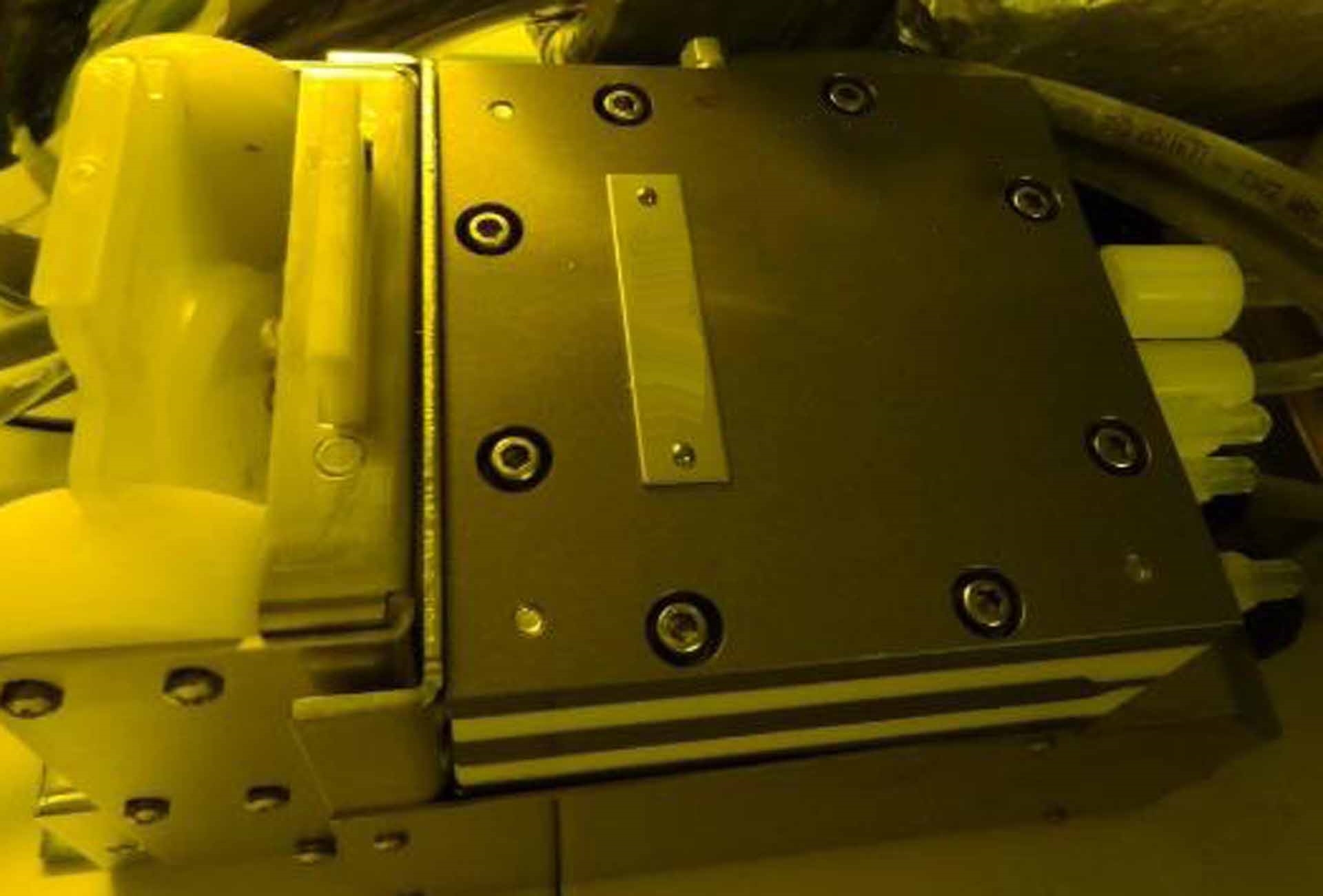

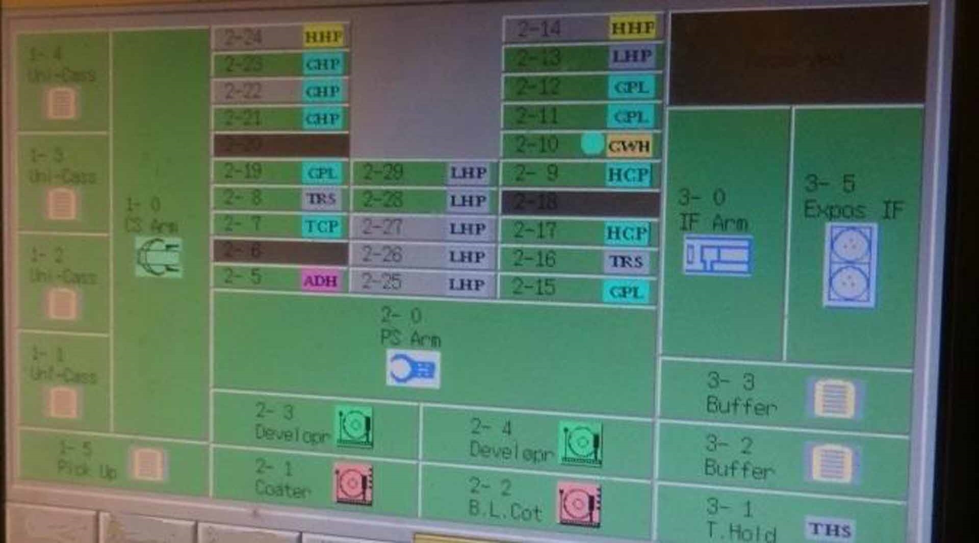


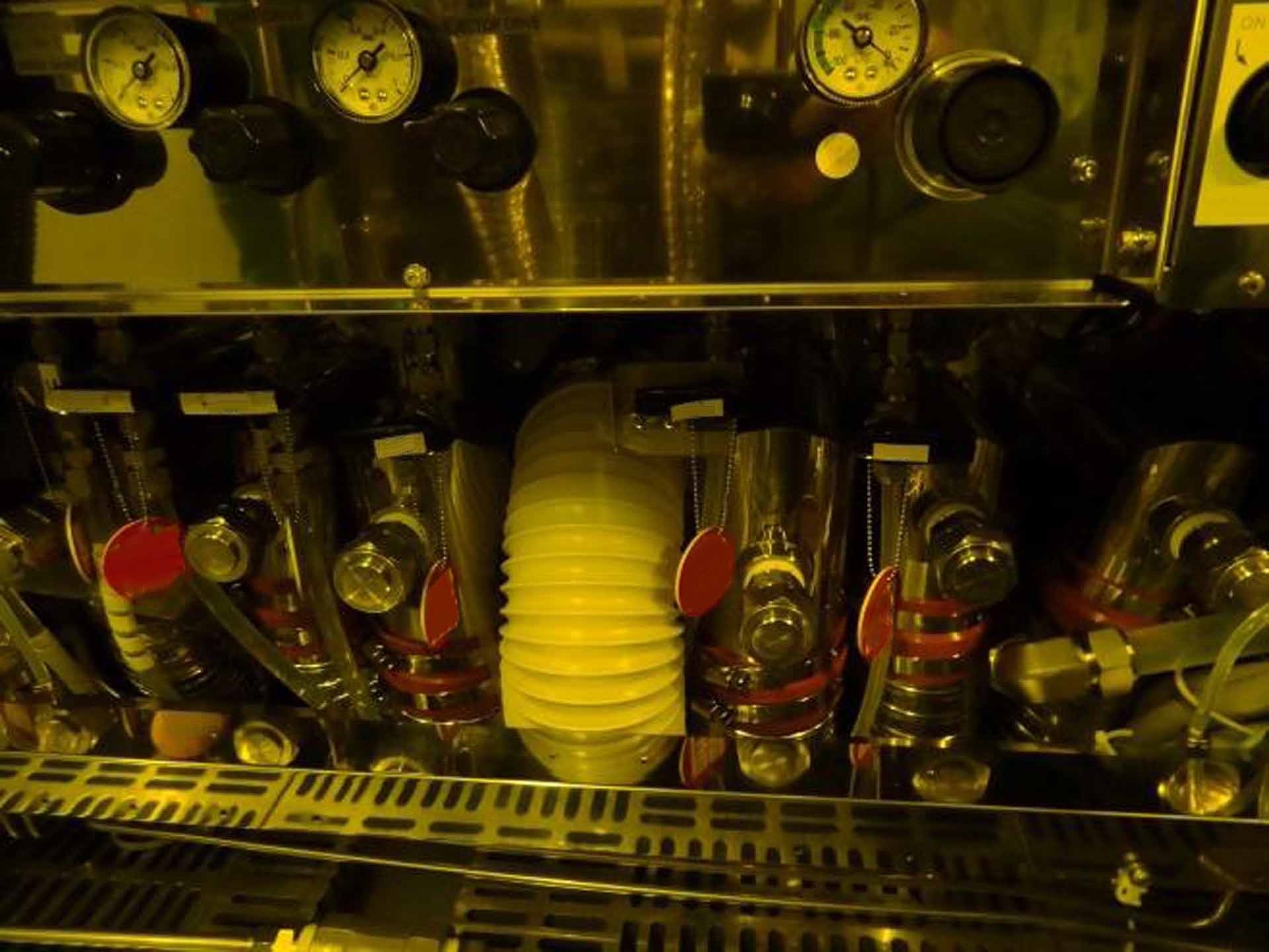

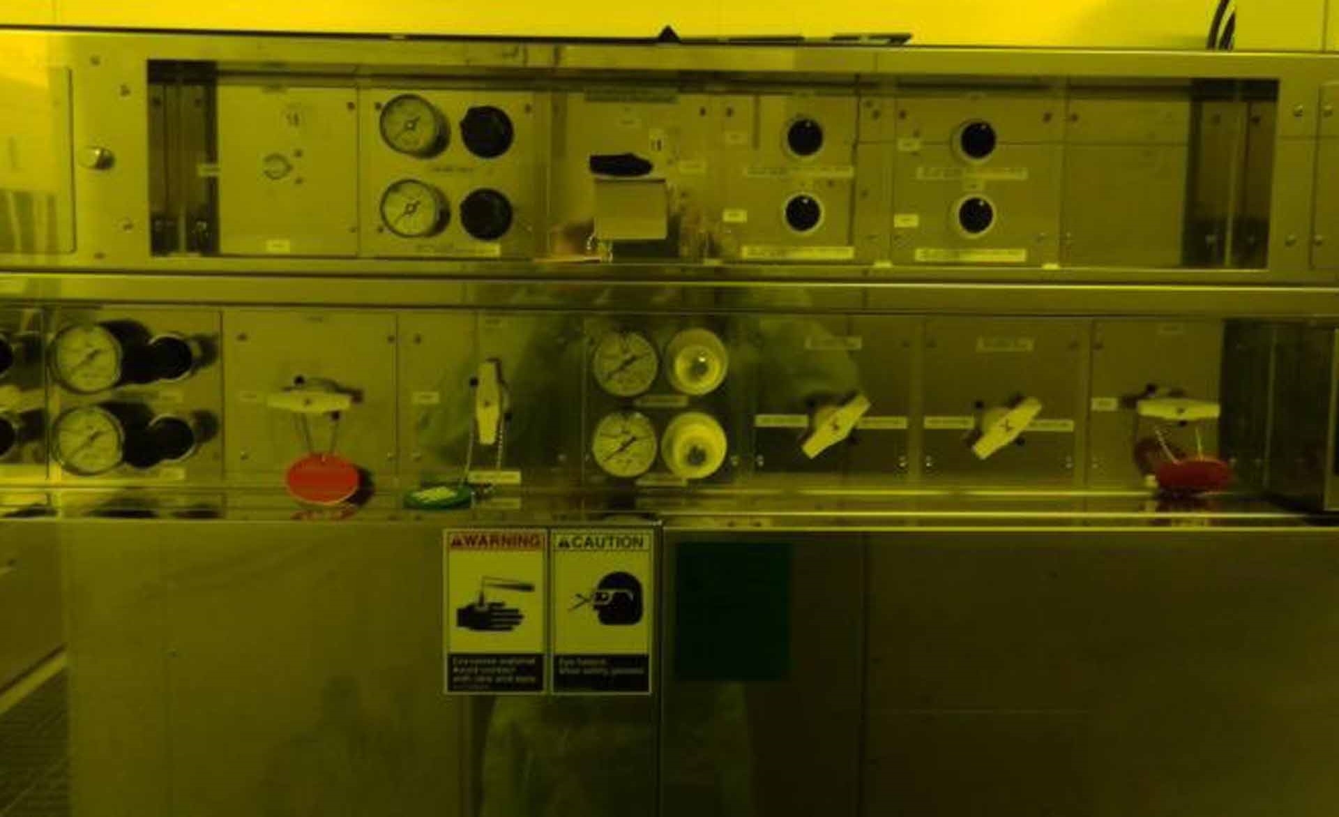

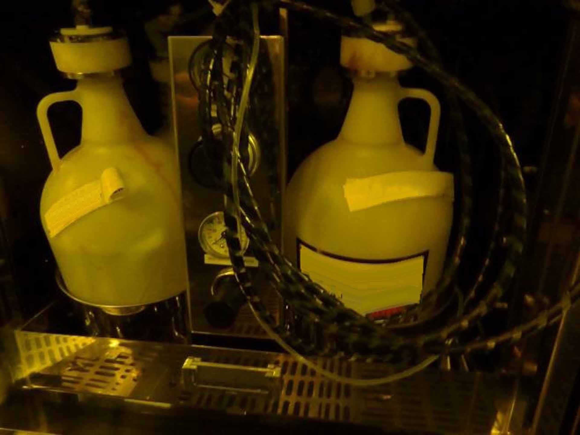

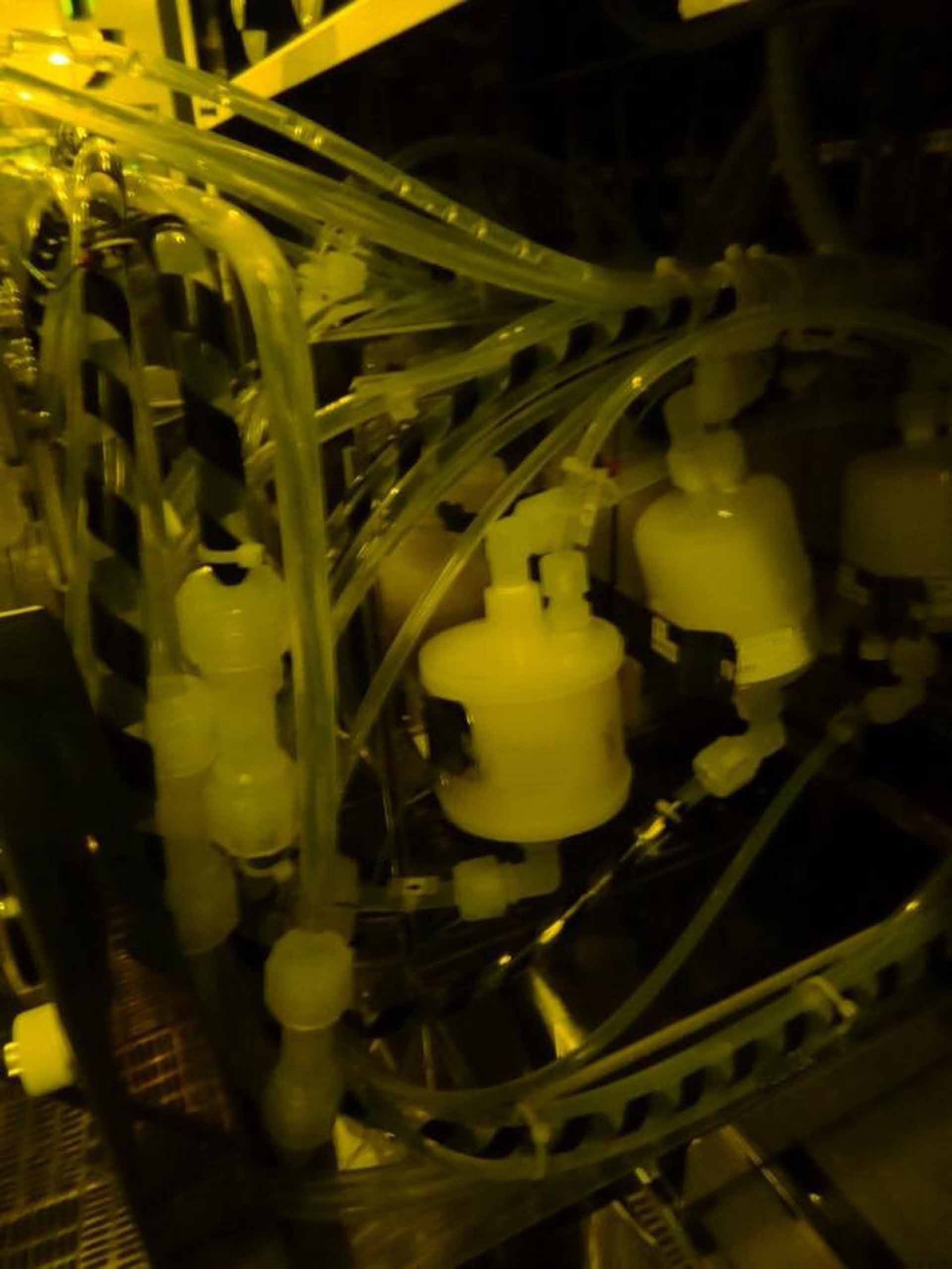

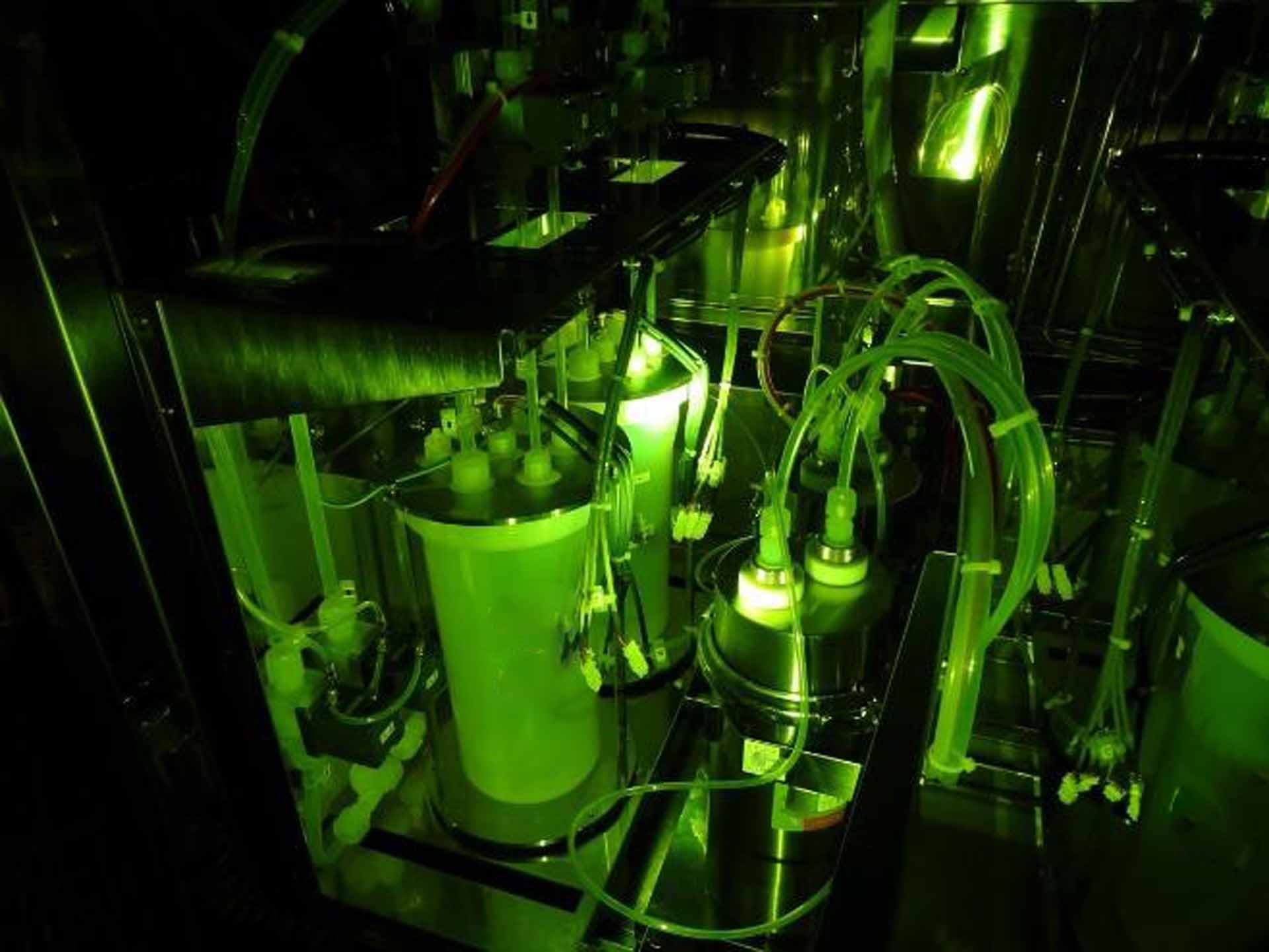

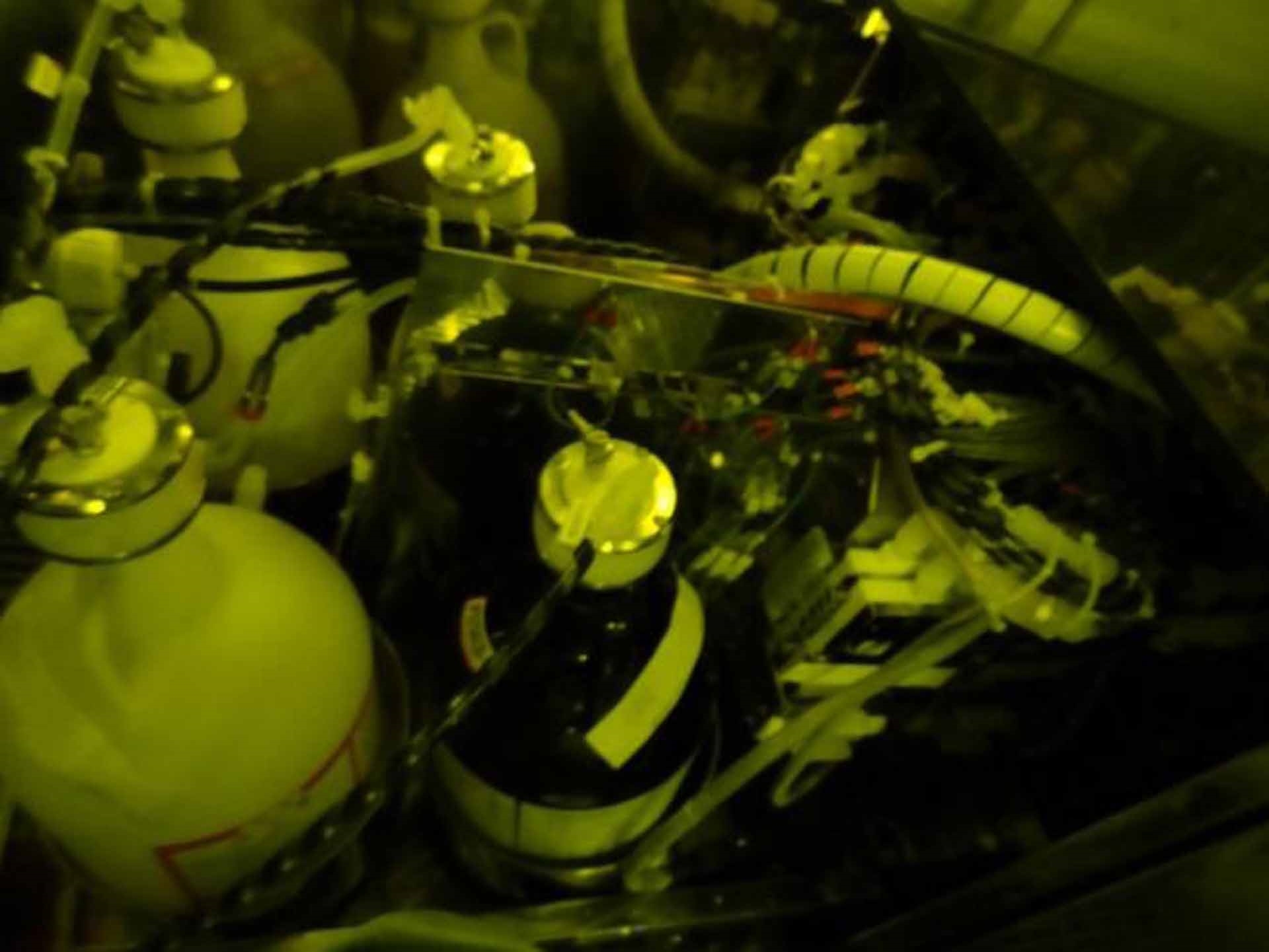

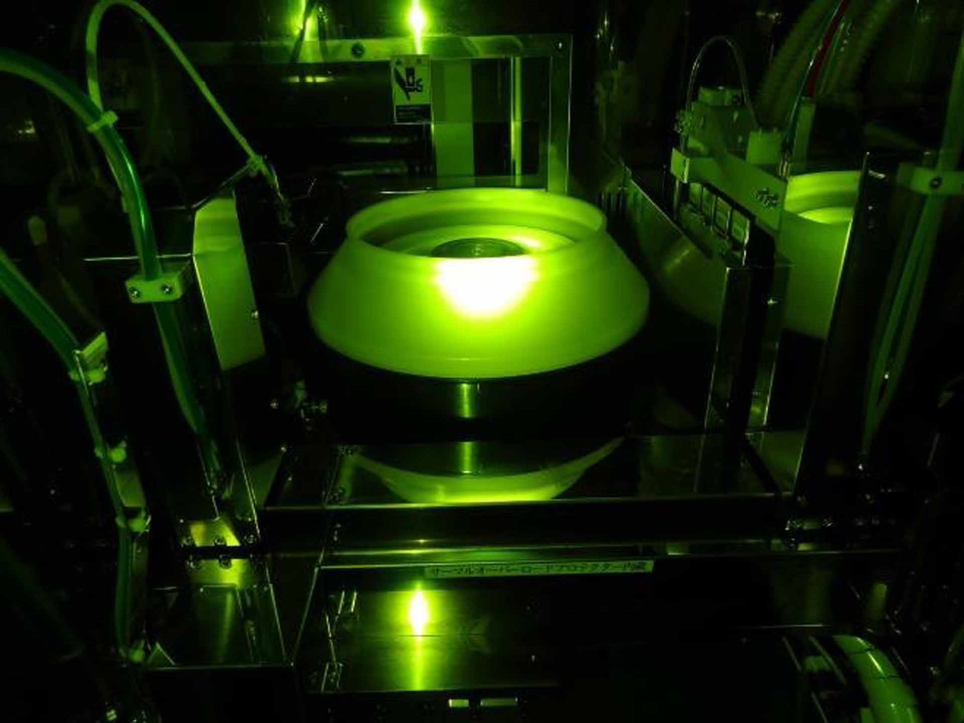

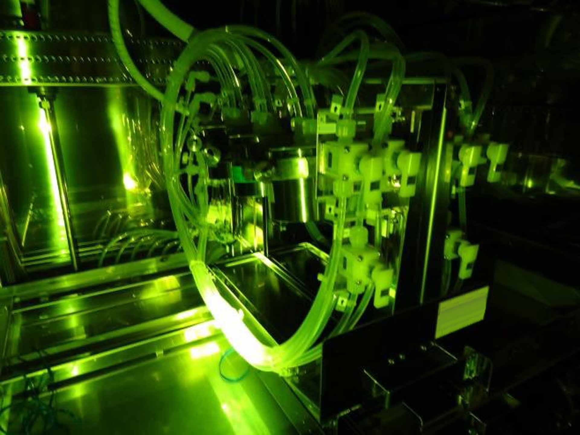

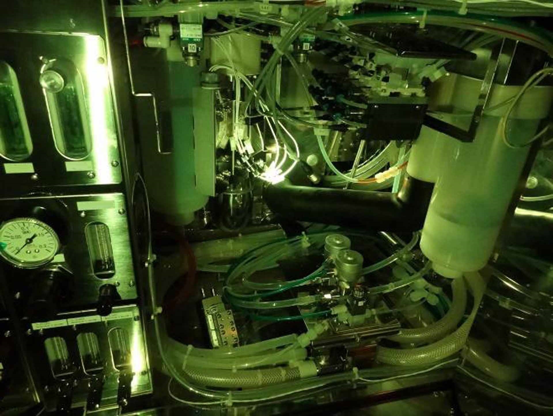

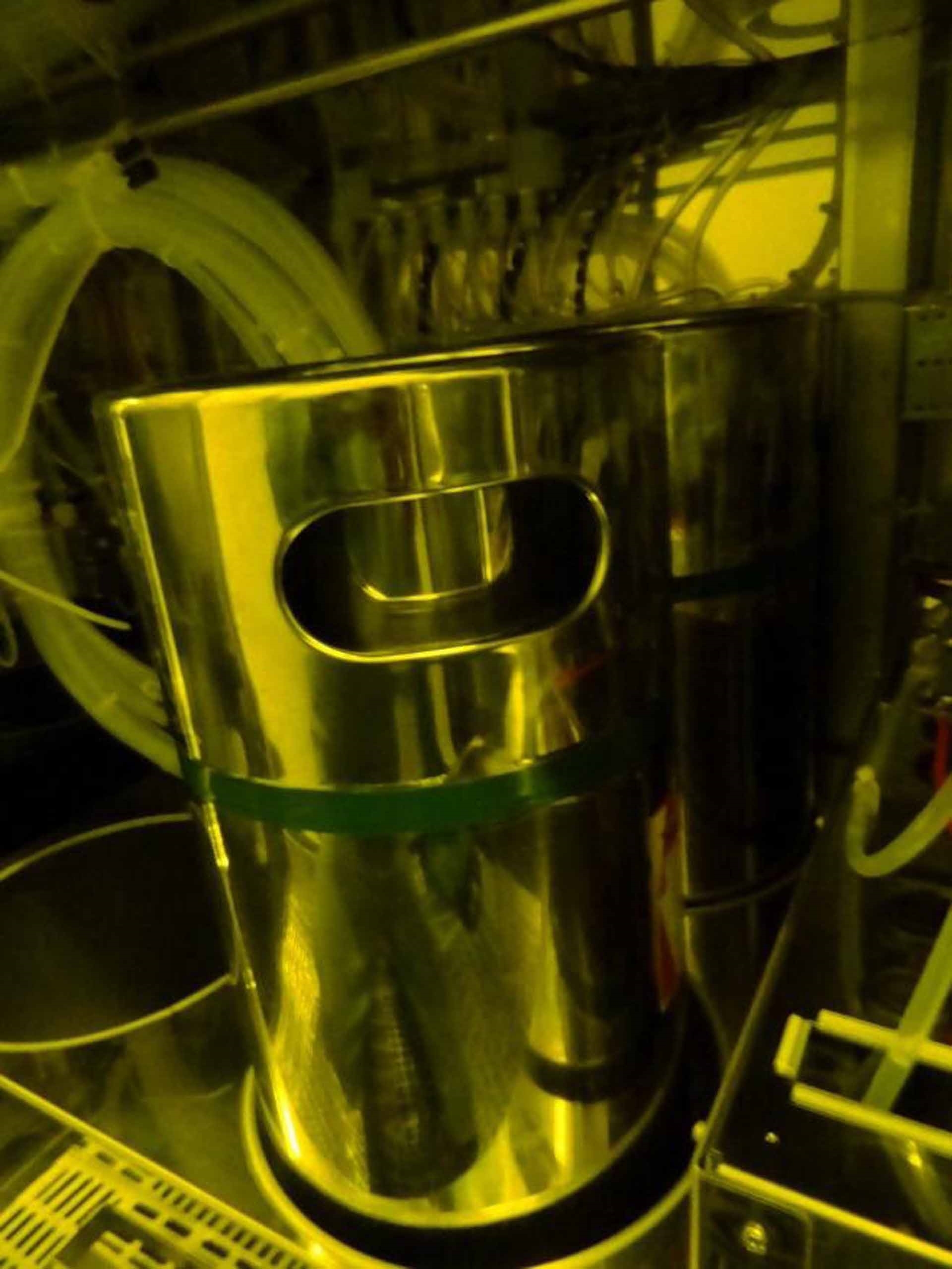

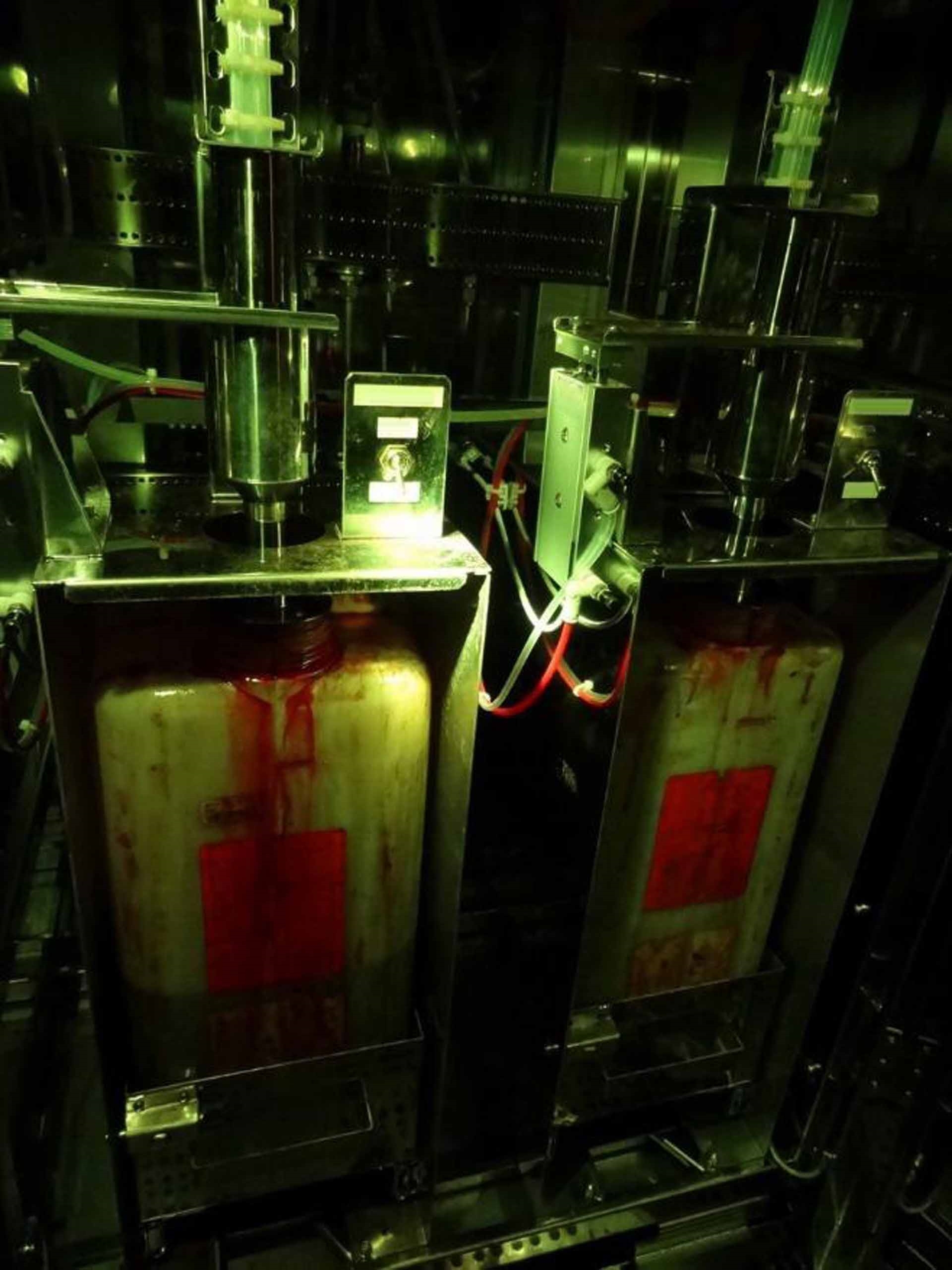

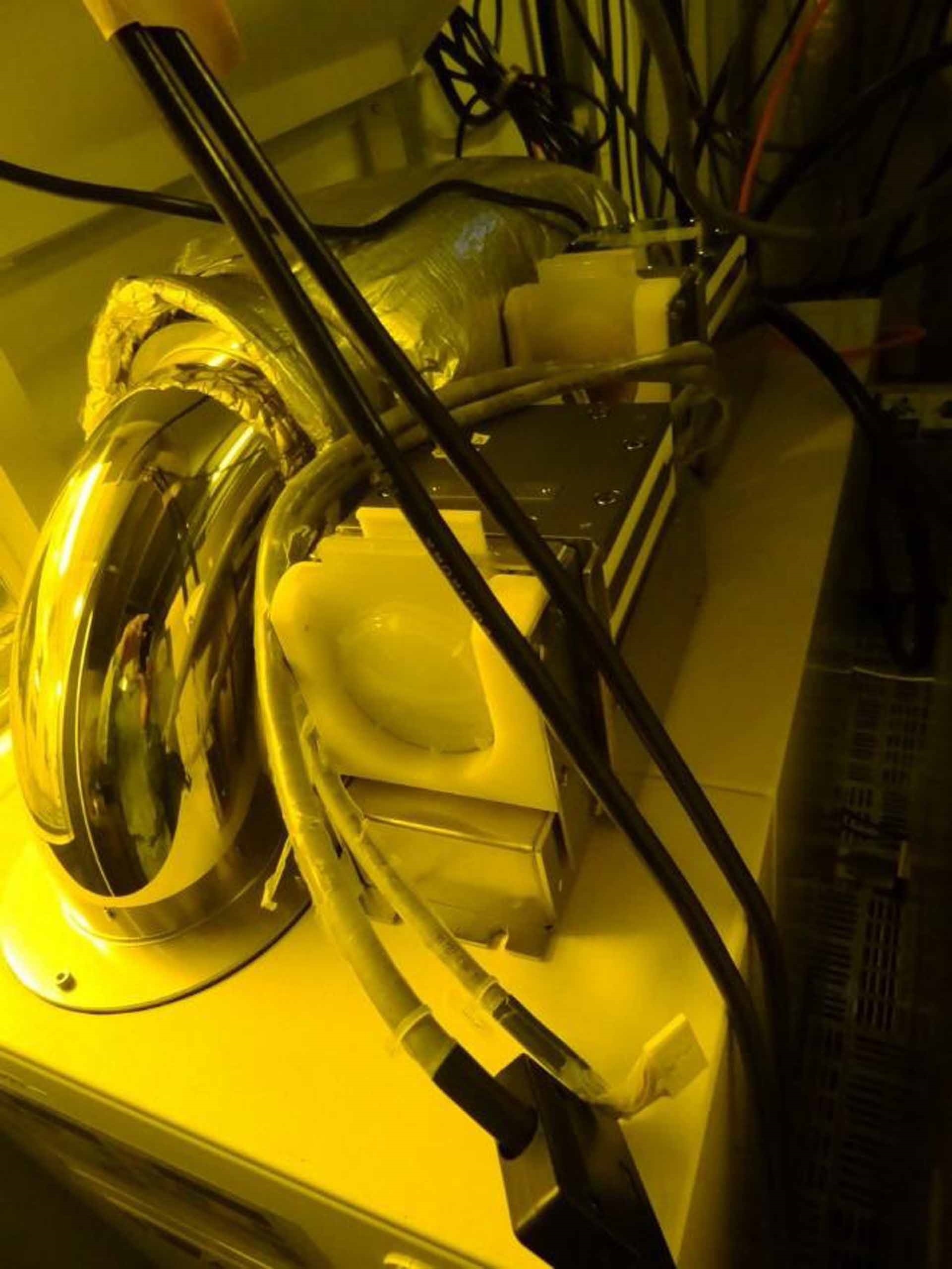

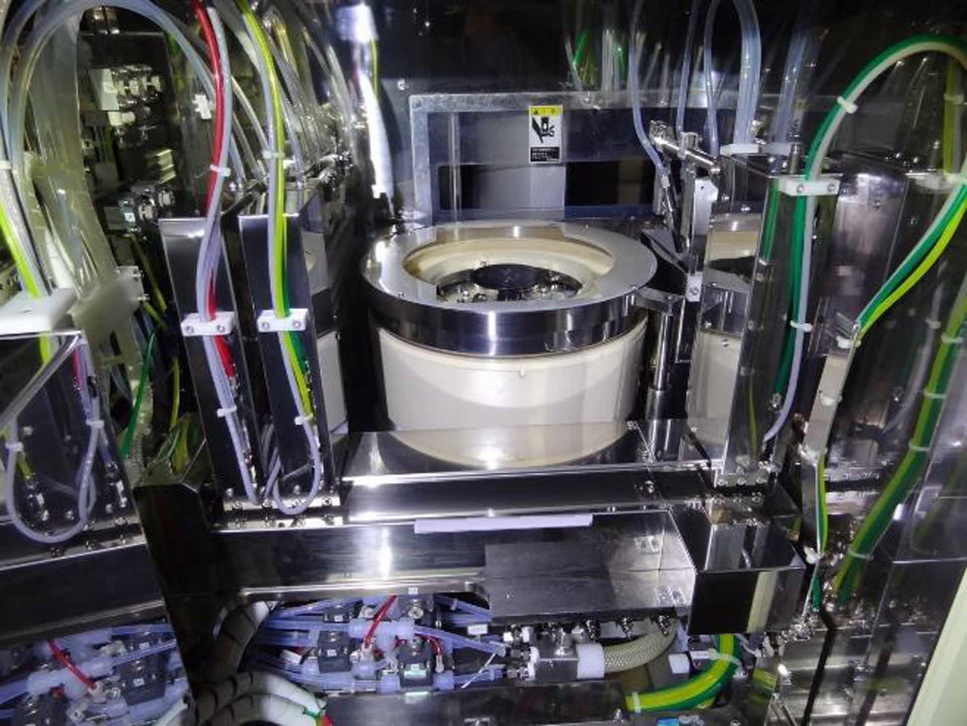

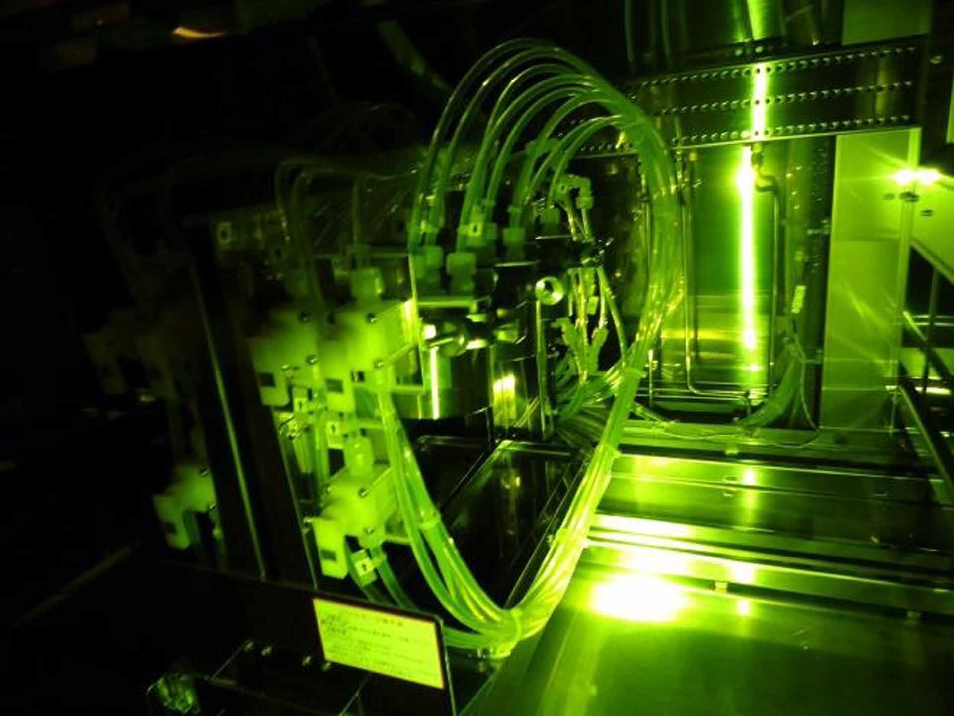


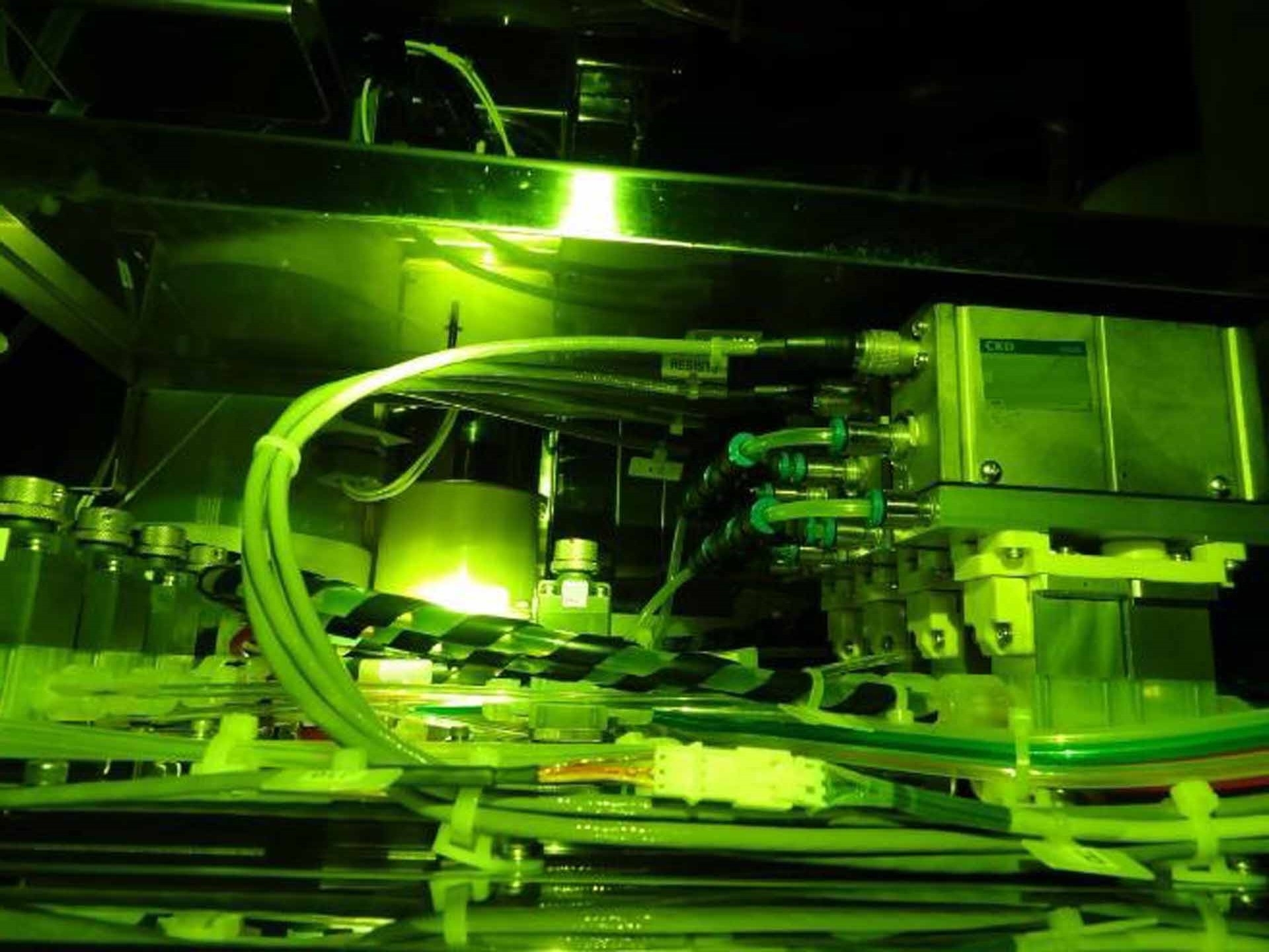


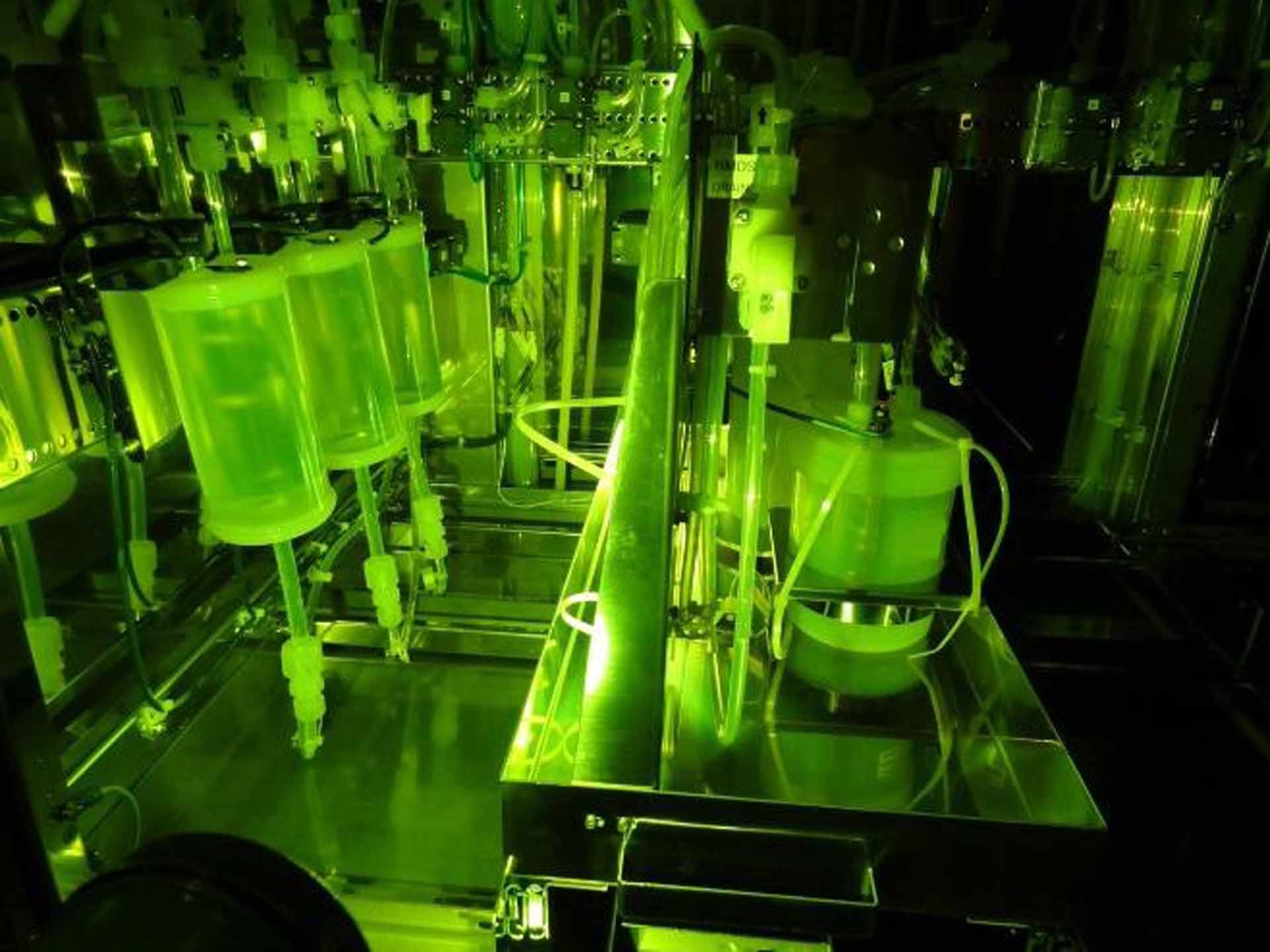

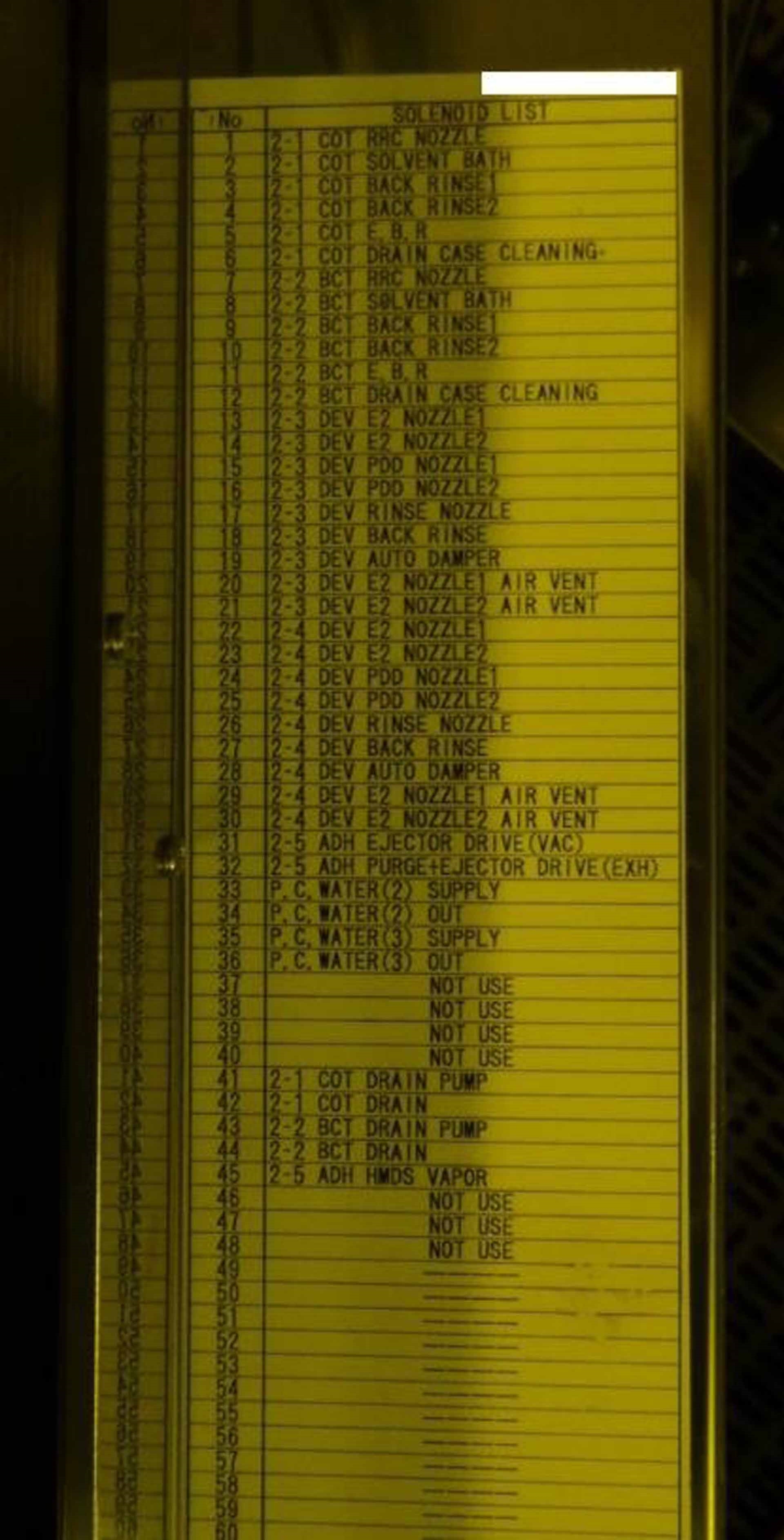


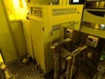
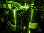
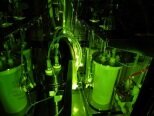
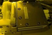
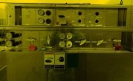
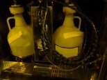
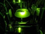
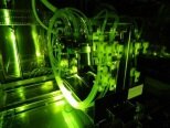
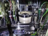
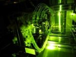
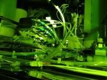
TEL / TOKYO ELECTRON ACT 8 photoresist equipment is an important tool in semiconductor processing. It is used to etch patterns into the surface of semiconductor wafers to form the electronic pathways, structures, and devices that make up electronic circuits and components. TEL ACT 8 photoresist system uses a photoresist, a light-sensitive material applied to the wafer's surface. When exposed to light, the photoresist changes its chemical composition and becomes a negative image of the pattern projected onto the wafer's surface. TOKYO ELECTRON ACT 8 unit allows a user to control the pattern definition, shape and size of the applied photoresist. The exposure time and intensity of the light can be set to match the specific chemical composition of the photoresist, allowing developers to precisely control features such as line width, resolution and even depth. ACT 8 machine also has several safety functions that protect against improper exposure of the photoresist. An algorithm is used to control the exposure duration so that incorrect exposure is avoided while ensuring the correct results. The tool is also equipped with a safety shutter that blocks out light during maintenance or while changing resist materials, further ensuring that the operator doesn't damage the wafer. The combination of features found in TEL / TOKYO ELECTRON ACT 8 photoresist asset makes it an ideal tool for photolithography development. The ability to control features and the safety measures help ensure that results are reliable and consistent. Furthermore, the 8th generation model adds flexibility and high-level automation, allowing for faster and more efficient photolithography processes.
There are no reviews yet

