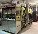
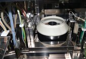
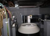
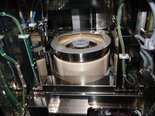
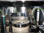
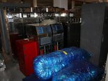
Used TEL / TOKYO ELECTRON Clean Track ACT 8 #9288585 for sale
URL successfully copied!
Tap to zoom


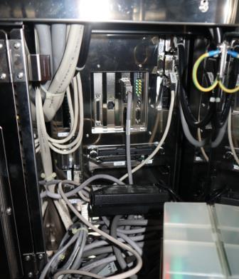

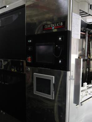

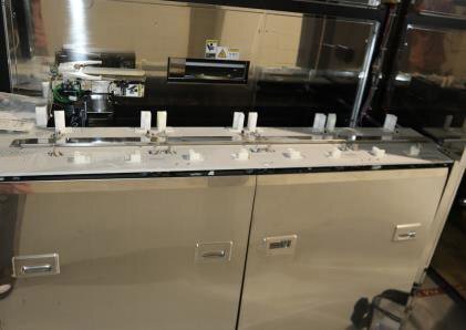


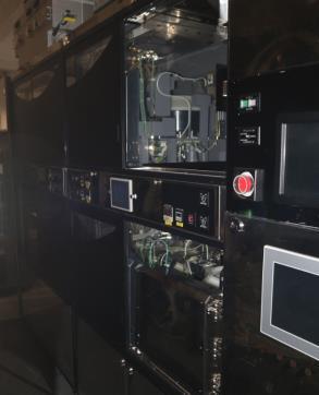

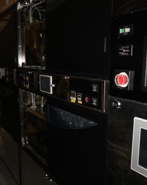

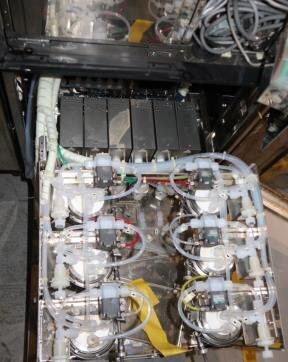

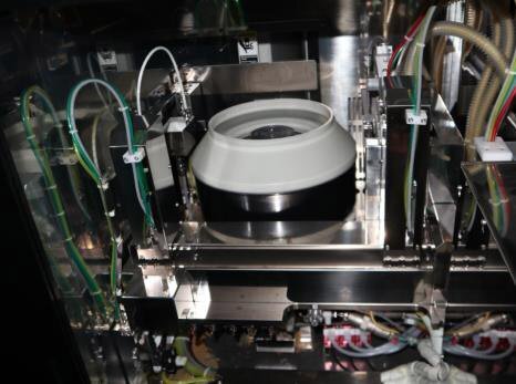












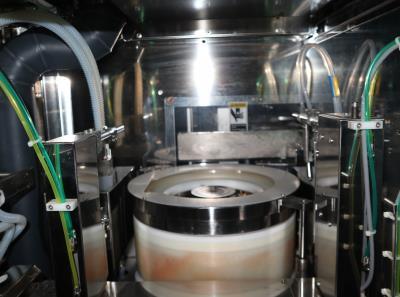

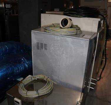

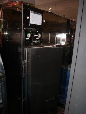

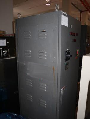




ID: 9288585
Wafer Size: 8"
Vintage: 2000
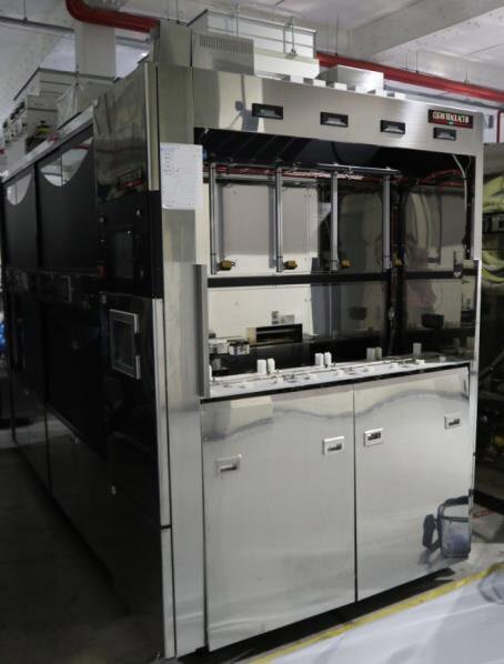
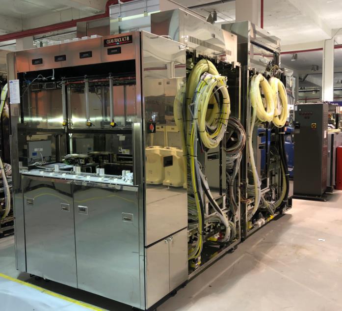
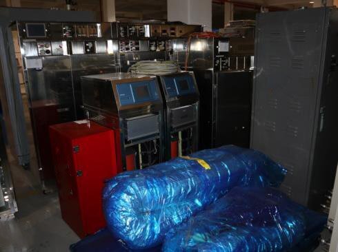
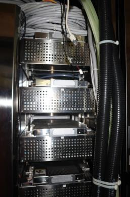
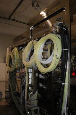
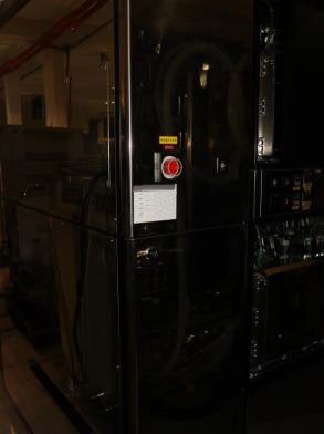
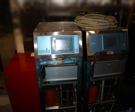
(3) Coater / (4) Developer system, 8"
Dual block
(4) Open cassettes: CSB
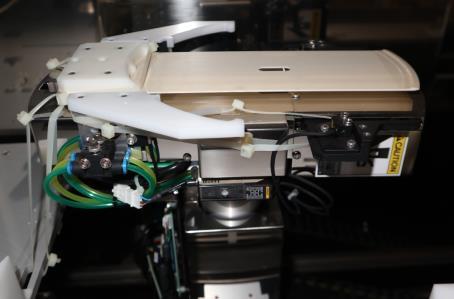
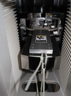
Transfer arm
Controller
Touch panel
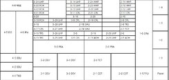
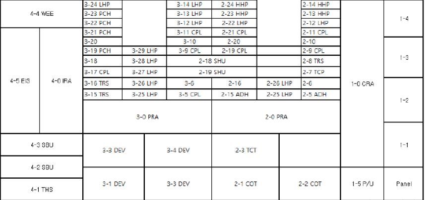
(2) Block bodies (SPIN: 3COT / 4 DEV)
RRC Pump: CSB
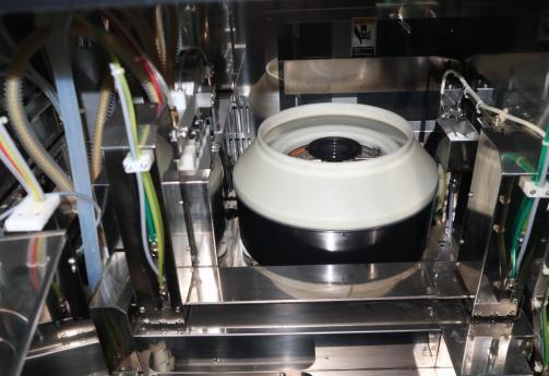
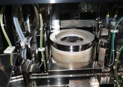
(3) COT Spin with 3 nozzles (2-1, 2-2: COT / 2-3 TCT)
Nozzle for DEV spin
Interface block:
WEE Unit
IFB Arm
Lamp house
Bake (1B, 2B):
(2) ADH
(8) CPL
(4) PCH
(13) LHP
(3) TRS
(4) HHP
Sub modules:
AC Power
(2) TCUs (SMC)
(2) Chemical cabinets
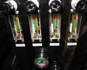
Cup temp / Humid (COSAM)
2000 vintage.
TEL / TOKYO ELECTRON ACT 8 is a photoresist equipment designed for precision photolithography. It is a customizable system that enables users to have optimum visibility and control over their production process. The unit features its own proprietary photoresist solution, which is an essential part of the photolithography process. This solution helps the user to apply the photoresist evenly over the target material in order to create a uniform and accurate result. At the heart of the machine is a proprietary laser-scanner that offers maximum precision and speed. It has an adjustable stage, with the ability to perfectly align it to any substrate size. The laser beam is focused at an extremely narrow width so that fine patterns can be accurately written onto the target material. The tool also features a patented automatic size-adjustment function ensuring that the exposure is precisely matched to the target shape. The asset is further enhanced by a built-in multiple exposure model. This allows users to expose the same pattern several times with different exposure settings. This equipment eliminates the need for manual pattern adjustment, ensuring consistent results every time. The system also includes a patented dielectric material latch designed for securing the photoresist onto the substrate. This feature ensures that the photoresist remains firmly attached to the substrate during the exposure process. Additionally, the unit features a programmable digital tilt machine which ensures that the photoresist is uniformly distributed over the substrate. The tool also features a comprehensive set of temperature and humidity sensors. This allows users to easily monitor and adjust the temperature and humidity to attain the precise conditions that will result in the desired resolution and clarity of the patterns. Finally, the asset also includes its own self-contained resist-developing model. This equipment removes the photoresist from the substrate after exposure, leading to the formation of the pattern. The system is equipped with sensors to ensure the precise pressure is applied to the substrate to achieve the optimal resist-removal results. Overall, TEL ACT 8 is an advanced photoresist unit designed for precision photolithography. Its combination of proprietary photoresist solution, laser-scanner, multiple exposure machine, and resist-developing tool gives it the ability to deliver the highest quality results in the shortest time possible.
There are no reviews yet

