Used TEL / TOKYO ELECTRON Clean Track ACT 8 #9312079 for sale
URL successfully copied!
Tap to zoom


ID: 9312079
Wafer Size: 8"
Vintage: 2007
(4) Coater / (4) Developer system, 8"
(2) Chemical boxes
(2) SMC Thermo controllers
TEAM KOREA Temperature and humidity controller
AC Power box
Left to right
Wafer and carrier type: Notch
(25) Slots
(4) Uni-cassette loaders
Carrier station:
Type: Normal uni-cassette
(4) Cassette stages
Pick-up cassette
Uni-cassette system
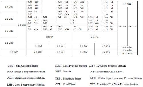
Coater unit (2-1, 2-2, 2-3, 2-4 Module):
(3) Dispense nozzles with temperature controlled line
RDS Pump
Rinse nozzle: Back / EBR / Solvent bath
Rinse system: 3 Liters (2) buffer tank systems
PR Suck-back valve type: AMC Suck-back valve
Programmable side rinse
Direct drain
Developer unit (3-1, 3-2, 3-3, 3-4 Module):
Nozzle for each unit
2-Stream nozzles for DI rinse
2-Points for back side rinse on each unit
Developer system: 3 Liters (2) buffer tank systems
Developer temperature control system
Direct drain
(2) Adhesion units:
Sealing closed chamber with built-in hot plate
HMDS Tank with float sensor
Interface type: NIKON
High temperature hot plate
(16) Low temp hot plates
(9) Chill Plates (CPL)
(4) Chilling Hot Plate (CHP) process station
(3) Transition Stage (TRS) modules
Transition Chill Plate (TCP) module
Wafer Edge Exposure (WEE) module
(2) Temperature control units
Missing parts:
Main controller
(4) Coater cups (2-1, 2-2, 2-3, 2-4)
(3) Developer cups (3-1, 3-2, 3-3)
Main display panel
CRA X-Axis motor
CSB Add on board
(9) Coater PR pumps (2-1.2-2.2-3)
IRA Y-Axis motor driver
IRA Tweezers
LHP Module cover
Power: AC 208 V, 3 Phase
2007 vintage.
TEL / TOKYO ELECTRON ACT 8 is an advanced exposure equipment designed for photoresist applications. It is a laser-driven system that uses high resolution and precise control of exposure times to reduce mask defects and increase consistency in the exposed photoresist image. This photoresist unit consists of a laser source, a modulator unit, a scanning unit, an analyzer unit, and a photoresist image detector. The laser source generates the photons used to expose the photoresist. This can be of a He-Cd or an argon-ion type. The modulator ensures that each laser pulse has exactly the same duration, permitting precise control of power density and providing a uniform 10ns exposure. The scanning machine utilizes a highly precise and rigid mechanical design to accurately expose the photoresist. It operates by scanning an XY motor-driven stage at 1.2 meters per second. The analyzer unit uses a CCD sensor to confirm exact exposure of the photoresist image. The photoresist image detector allows for deflection-independent measurement of extremely accurate resist patterns. It combines a stage for measurement, a control unit for data input, and a display unit for signal output. It can detect positional errors as small as 0.2 micrometres. TEL ACT 8 is suitable for use in a variety of industries such as semiconductor manufacturing. It enables chipmakers to quickly and accurately produce devices with improved resolution and eliminates mask flipping. This advanced tool is capable of achieving a printing accuracy of 0.1 micrometres. It also offers excellent resource utilization with its ability to process large products at high speed.
There are no reviews yet