Used TEL / TOKYO ELECTRON Clean Track ACT 8 #9312222 for sale
URL successfully copied!
Tap to zoom


ID: 9312222
Wafer Size: 8"
Vintage: 2001
Coater / Developer system, 8"
Main frame with system controller
Carrier station:
Type: Normal uni-cassette
4-Cassette stages
Pick-up cassette
Coater unit:
(3) Dispense nozzles
With temperature controlled line
RRC Pump
Rinse nozzle: Back / EBR / Solvent bath
Rinse system: 3 Liters (2) Buffer tank systems
P.R Such-back valve type: Suck-back valve
Direct drain
TARC Coater unit:
(2) Dispense nozzles
With temperature controlled line
RRC Pump
Rinse nozzle: Back / EBR / Solvent bath
Rinse system: 3 Liters (2) buffer tank systems
P.R Such-back valve type: Suck-back valve
Direct drain
Developer unit:
SH Nozzle
(2) SH Nozzles for DI Rinse
2-Points for back side rinse
Developer system: 3 Liters (2) buffer tank systems
Developer temperature control system
Direct drain
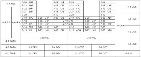
(3) Adhesion units:
Sealing closed chamber (Built-in hot plate)
HMDS Tank with float sensor system
Interface
(15) Low temp hot plates
(14) Chill plates (CPL)
(3) TRS Module
TCP Module
Wafer Edge Exposure (WEE) Module
Wafer type: Notch, DUV Type
(2) Chemical cabinets:
Chemical cabinet 1: Solvent and developer
Chemical cabinet 2: HMDS and PR
(2) Temperature Control Units (TCU)
AC Power box
Missing parts:
2-1 COT Spin I/O Board
2-4 COT EBR Nozzle tip
2-4 COT EBR Nozzle valve
2-1 Nozzle changer motor
3-2 Shutter cylinder
(2) PRB YASUKAWA Spin motor drivers
2-0 PRA Z-Driver
3-0 PRA Z-Driver
Temperature and humidity controller (For 4 chu)
Hard Disk Drive (HDD)
2001 vintage.
TEL / TOKYO ELECTRON ACT 8 is a photoresist equipment developed by TEL in partnership with Canon Electronics. It is a next-generation technology that combines the high-performance capabilities of a single-beam or dual-beam deep-ultraviolet (DUV) laser lithography system with advanced resist technologies. The core parts of this unit are a deep-ultraviolet laser, resist processor, and fine-alignment stage. The deep-ultraviolet laser emits a beam at a wavelength of 248nm, making it ideal for creating extremely small features on the printed wafer. It can also process up to eight layers simultaneously, providing a significant increase in productivity. The integrated resist processor and fine-alignment stage provide precision control over the entire photolithography process. In addition, TEL ACT 8 has been designed to minimize production cycle times. TOKYO ELECTRON ACT 8 also incorporates several advanced features. It is capable of achieving a resolution as small as 12nm in a single pass, allowing for the creation of highly intricate circuit patterns. The machine also includes dynamic focus capabilities, enabling the correction of any misalignments during the exposure process. In addition, TEL / TOKYO ELECTRON ACT 8 features a sophisticated recipe management tool, an intuitive user interface, and precise uniformity control. ACT 8 is highly reliable and able to maintain the desired resolution for up to 100 wafers. TOKYO ELECTRON has performed intensive reliability tests to ensure superior performance in even the most extreme conditions. The asset meets the requirements of top international semiconductor companies and has been adopted by many of them around the world. The photoresist model can be employed in a wide range of industries, from electronics to automotive parts and medical devices. TEL ACT 8 offers unmatched precision and is well-suited for tasks demanding very fine detail, such as in micro-LEDs and micro-resistors. The equipment is also fast, efficient, and reliable, making it ideal for high-volume production runs. No matter the requirements, ACT 8 provides the highest quality results with minimal downtime. The combination of precision, efficiency, and reliability makes it the perfect choice for any application demanding the highest level of performance.
There are no reviews yet