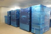
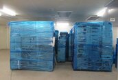
Used TEL / TOKYO ELECTRON Clean Track ACT 8 #9383672 for sale
URL successfully copied!
Tap to zoom


ID: 9383672
Vintage: 1995
Coater / Developer system
COT
TCT
(3) DEV
WEE
Missing parts:
WEE VAC Solenoids and light guide set
DEV Spin motor driver
AC Power box
AC Control box
Tweezers for WAF Guide fixing screws
IAZ Axis driver
IRAθ Axis driver
Cup temperature and humidity machine:
Wiring pipe
Drain pan
Leak sensor for drain pan
1995 vintage.
TEL / TOKYO ELECTRON Clean Track ACT 8 is an automated photoresist equipment designed for use in the semiconductor industry. The system is used to precisely etch patterns into semiconductor materials. The unit is comprised of multiple components that work together to manipulate the photoresist material. The first component is a Photoelectron Mask Aligner (PMA), which is responsible for accurately placing the desired pattern onto the wafer material. The PMA then uses ultraviolet (UV) light to transfer the pattern onto the photoresist. This step is called 'exposure'. The second component is a chemical processing station, which is responsible for removing the exposed portions of the photoresist. This step is usually done by applying a water-based, alkaline solution to the photoresist. This process is known as 'developing'. The third component is a spin drier, which is used to dry the material after the developing step. This step ensures that the next step, etching, can be carried out correctly. The fourth component is an etcher, which is used to etch the desired pattern into the material. Depending on the material being etched, this can be done with dry etching, wet etching, or plasma etching. The fifth component is a lift-off station, which is responsible for removing the remaining photoresist from the etched pattern. This is usually done with a chemical lift-off agent which breaks the chemical bonds between the photoresist and the material. The sixth component is an Alignment Mark Inspection (AMI) station, which is used to inspect the alignment accuracy of the etched pattern. This ensures that the etched pattern meets the design specifications. The seventh component is a cleaning station, which is used to remove any remaining photoresist, chemical agents, or particles from the wafer material. This helps to ensure that the semiconductor is free from contamination. Finally, the eighth component is a transport station, which is responsible for moving the wafer material to the next step in the process. TEL Clean Track ACT 8 is an essential component in the semiconductor fabrication process, as it enables the precise and accurate fabrication of semiconductor materials. By combining the PMA, chemical processing station, spin drier, etcher, lift-off station, AMI, cleaning station, and transport station into a single machine, TOKYO ELECTRON Clean Track ACT 8 simplifies the process of fabricating semiconductor materials.
There are no reviews yet

