Used TEL / TOKYO ELECTRON Clean Track Mark VII #293760424 for sale
URL successfully copied!
Tap to zoom
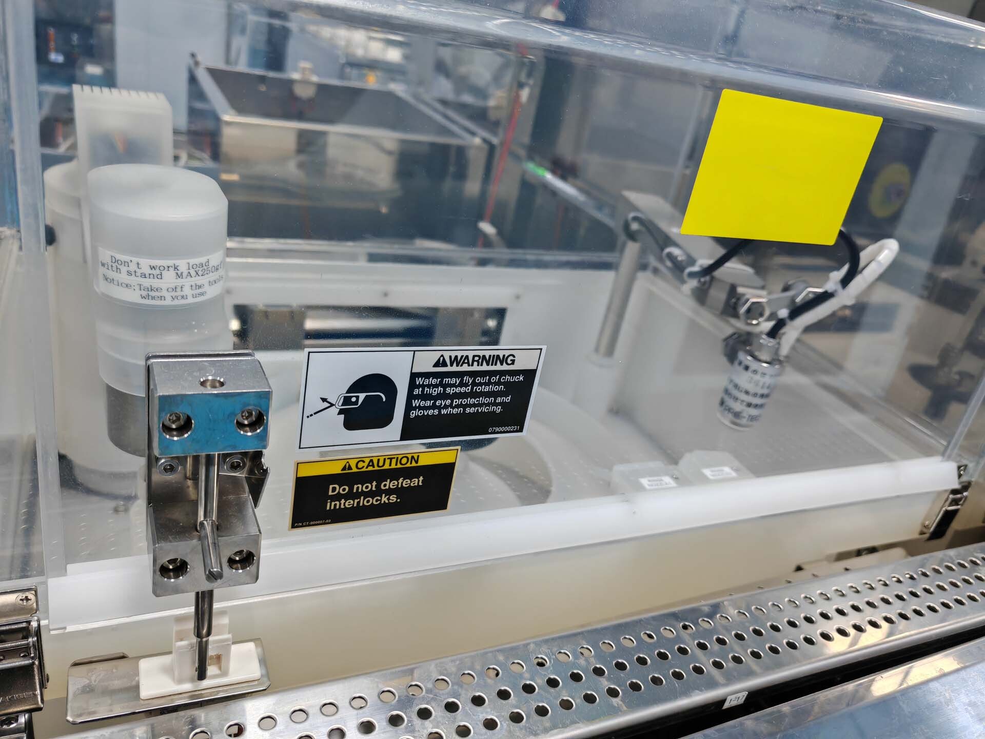

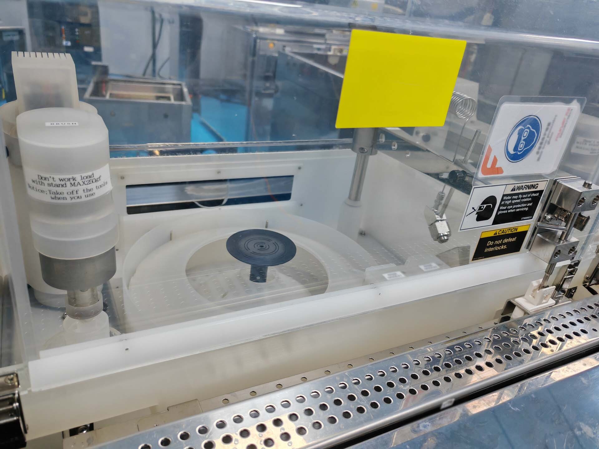
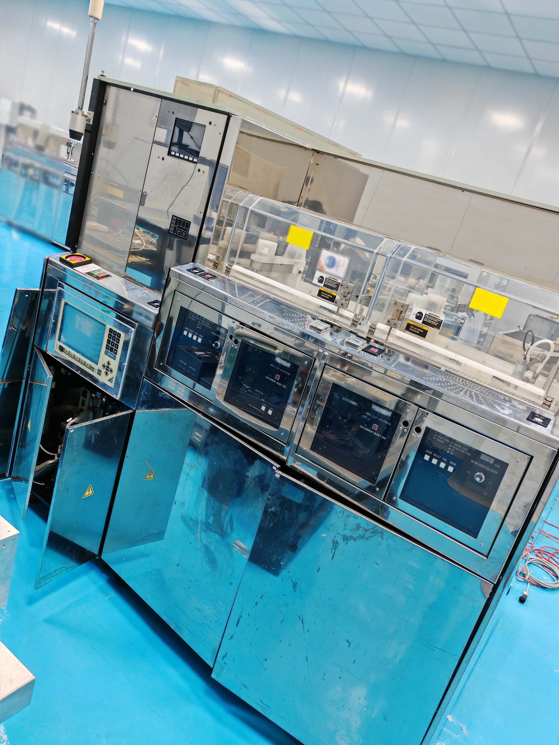
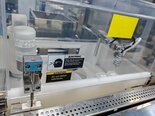
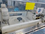
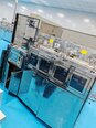
TEL / TOKYO ELECTRON Clean Track Mark VII is a sophisticated photoresist processing equipment used in the semiconductor industry for advanced lithography processes. This system is designed to provide precise and consistent application of photoresist materials onto silicon wafers, a critical step in the production of semiconductor devices. At the heart of the Mark VII unit is its advanced robotic handling machine, which allows for automated loading and unloading of wafers, ensuring minimal human intervention and reducing the risk of contamination. This automation feature also enables high throughput and efficiency in processing, making the tool ideal for high-volume manufacturing environments. The Mark VII asset is equipped with a range of modules and subsystems that work together to deliver precise and reliable photoresist processing capabilities. One key component of the model is the spin coating module, which applies a uniform layer of photoresist material onto the wafer surface. The spin coating process involves dispensing a predetermined amount of photoresist material onto the center of the spinning wafer, creating a thin and even coating that is essential for producing high-quality semiconductor devices. After the photoresist material has been deposited onto the wafer, the Mark VII equipment utilizes a sophisticated baking module to thermally cure the photoresist layer, ensuring proper adhesion to the wafer surface and minimizing defects. The baking process is carefully controlled to optimize the properties of the photoresist material, such as its thickness and chemical composition, to meet the specific requirements of the lithography process. In addition to the spin coating and baking modules, the Mark VII system also incorporates a development module, which facilitates the removal of unwanted photoresist material from the wafer surface. The development process involves immersing the wafer in a chemical solution that selectively dissolves the exposed photoresist material, leaving behind a patterned layer that can be used for subsequent etching and deposition steps in the semiconductor manufacturing process. The Mark VII unit is designed to operate in a cleanroom environment to minimize the risk of contamination and ensure the integrity of the semiconductor devices being produced. The machine is equipped with advanced filtration and purification systems to maintain the purity of the chemicals used in the photoresist processing steps, as well as to control the ambient temperature and humidity levels for optimal processing conditions. Overall, TEL Clean Track Mark VII is a state-of-the-art photoresist processing tool that offers advanced capabilities for precise and reliable semiconductor manufacturing. With its automated handling, precise coating and baking processes, and cleanroom compatibility, the Mark VII asset is an essential tool for semiconductor manufacturers seeking to produce high-quality devices with tight tolerances and advanced functionality.
There are no reviews yet