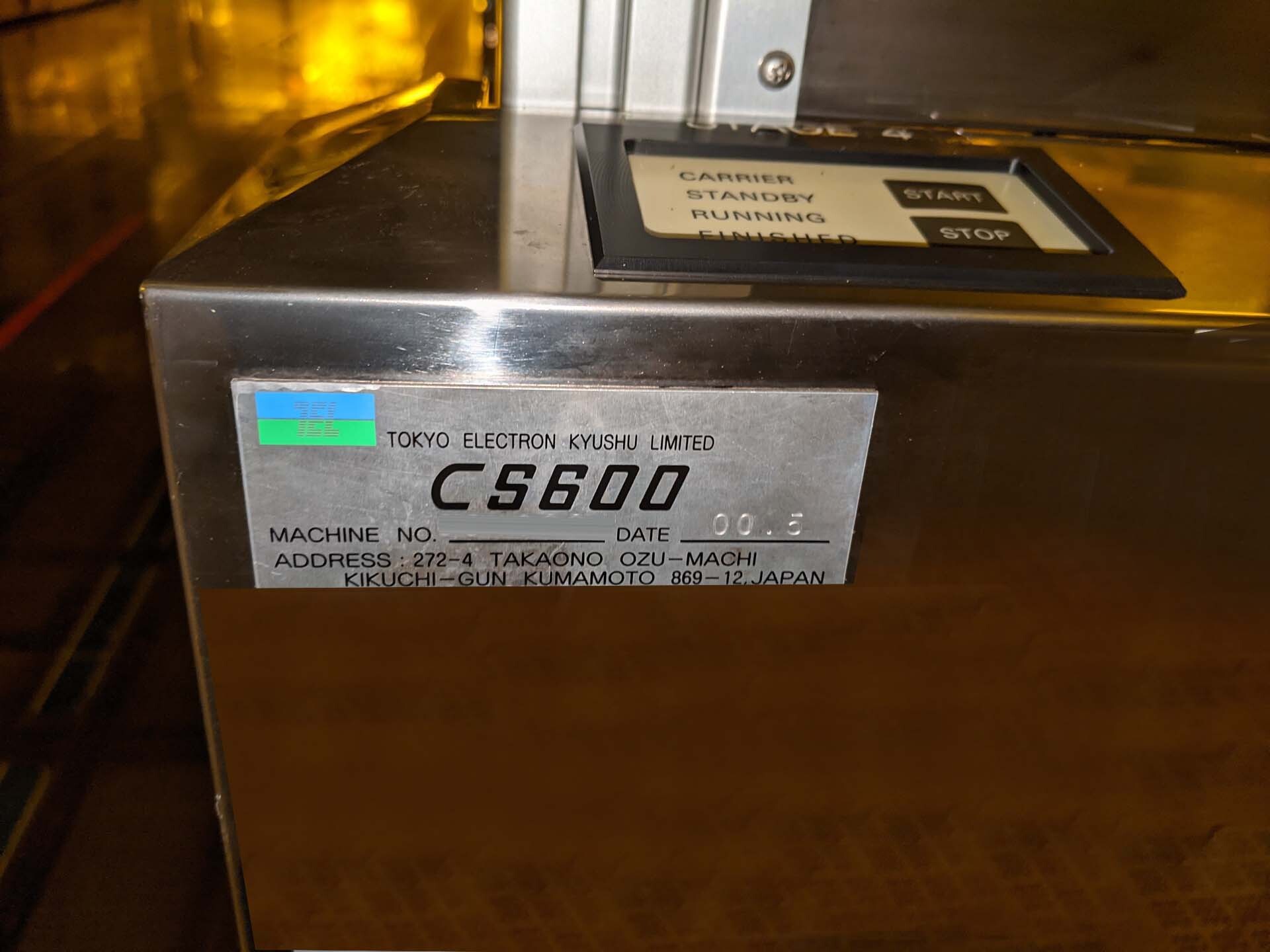
Used TEL / TOKYO ELECTRON CS-600 #9380665 for sale
URL successfully copied!
Tap to zoom


TEL / TOKYO ELECTRON CS-600 photoresist equipment is a comprehensive process system designed primarily for lithography patterning of advanced photoresist materials on wafers from 300mm to 200mm. It supports the processing of multiple multi-layer photoresists and enables processing at a high precision with 30nm repeatability. It contains simultaneous height/focus/dose metrology which provides precise focus and dose control for high-accuracy patterning and also features a direct optical-pattern imaging unit for exact pattern placement. TEL CS-600 machine uses an Optical Thermal Projection (OTP) of high resolution images to achieve precise photoresist patterning processes. OTP utilizes advanced projection optics and imaging technology with Pupil Imaging (PI) and the Feature Brightness Compensation (FBC) to bring a high intensity, homogenous mask image onto the resist film. This enables a variety of patterning techniques such as off-center exposure, bottom anti reflection layer (BARL) processing, and attenuated patterning in multi-layered processes. The PI technique allows for superior resolution of the pattern elements and the FBC compensates for the difference in brightness of the pattern elements due to their size. TOKYO ELECTRON CS-600 offers high frequency (up to 300kHz) opto-acoustic scanning which provides high precision, high speed, and high resolution patterning. They are also capable of performing sub-micron alignment of wafer planes for pattern transfers and a variety of alignments, as well as support for advanced imaging and resist masking features. The temperature control feature of CS-600 offers a uniform resist film thickness for consistent patterning results. It is capable of handling various processes such as top side baking, coating, baking, and exposure. The extremely low temperature setting of TEL / TOKYO ELECTRON CS-600 also helps to minimize the possibility of resist damage during the process. In addition to the universal resist processing process, TEL CS-600 is also capable of processing a variety of advanced photoresist materials. It is designed to handle single layer and multi-layer photoresist applications. TOKYO ELECTRON CS-600's rapid optical imaging tool allows the user to image photoresist features with 0.2um accuracy. The photoresist asset is also equipped with advanced analytic control and inspection processes. These include design rule checking, topography measurement, exposure dose control, resolution measurement, defect inspection, contamination inspection, wafer/pixel uniformity measurement, and particle metrology. CS-600 offers outstanding performance for lithography patterning and is a highly reliable model for handling sophisticated photoresist processes. It is extremely costly, making it difficult for many labs to acquire, but overall TEL / TOKYO ELECTRON CS-600 provides the highest level of photoresist performance available today.
There are no reviews yet