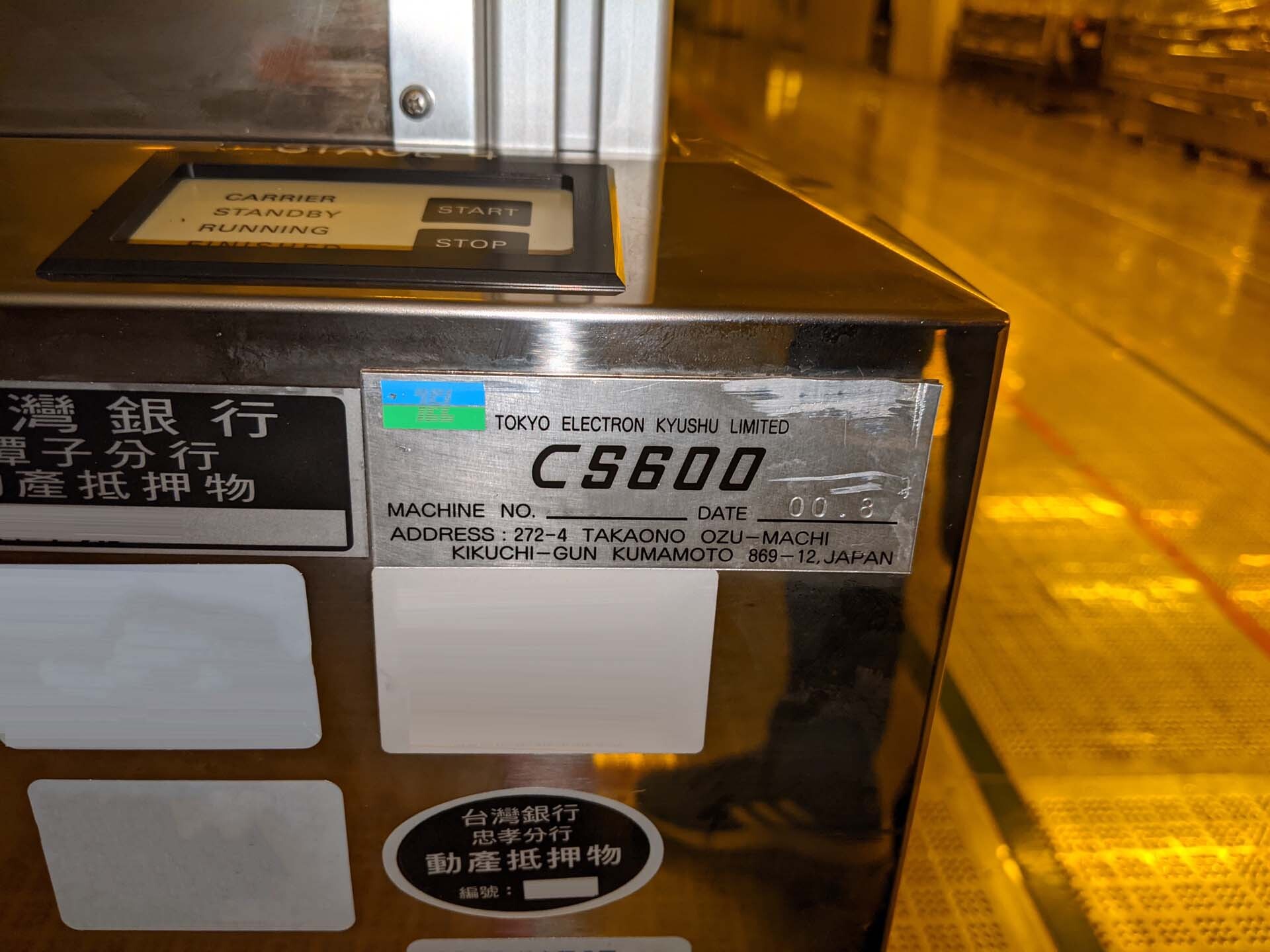
Used TEL / TOKYO ELECTRON CS-600 #9380675 for sale
URL successfully copied!
Tap to zoom


TEL / TOKYO ELECTRON CS-600 photoresist equipment is a monolithic lithography system designed for exposure of photoresist material with minimal pattern deformation. It offers superior dielectric uniformity, allowing for finely detailed features to be printed with extreme accuracy and superior yields when compared to traditional lithography exposure systems. The unit integrates a variety of features, including an advanced high-frequency mask holding machine, auto-focus, and laser alignment. TEL CS-600 offers a stage accuracy of 10nm, allowing for high precision patterning of resists on the order of critical features. To maintain this accuracy, TOKYO ELECTRON CS-600 employs a high-precision linear motor stage drive tool that compensates for thermo-mechanical variation in order to ensure repeatable high-accuracy exposures. The asset's high-frequency mask holding model supports dielectric 5-500nm thick mask sets, allowing for intricate, fine features of the photoresist material to be accurately exposed. CS-600's laser alignment equipment ensures alignment of the photomask relative to the substrate, providing a stable patterning process for high resolution results. The system's auto-focus feature ensures nano-scale accuracy throughout the exposure process. By utilizing a patented high-resolution laser diode, TEL / TOKYO ELECTRON CS-600 can measure the critical edge of the photoresist pattern and automatically adjusts its focus. This results in consistently accurate patterns even when the substrate's topography or roughness changes. TEL CS-600 also offers a variety of high-end features, such as ultra-high resolution resolution imaging at 5nm in both wavelength and numerical aperture. This results in a high throughput performance and an extremely low defect rate. TOKYO ELECTRON CS-600 is an accurate, easy-to-use, reliable photoresist unit that is designed to address the challenges of the ever-evolving microelectronics industry. It has the capability to achieve edge resolution down to 5nm with high accuracy repeated exposures, allowing for high resolution patterns to be printed with superior yields. As such, it is an ideal solution for advanced and high-volume microelectronics applications.
There are no reviews yet

