Used TEL / TOKYO ELECTRON ECC2 #293804699 for sale
URL successfully copied!
Tap to zoom
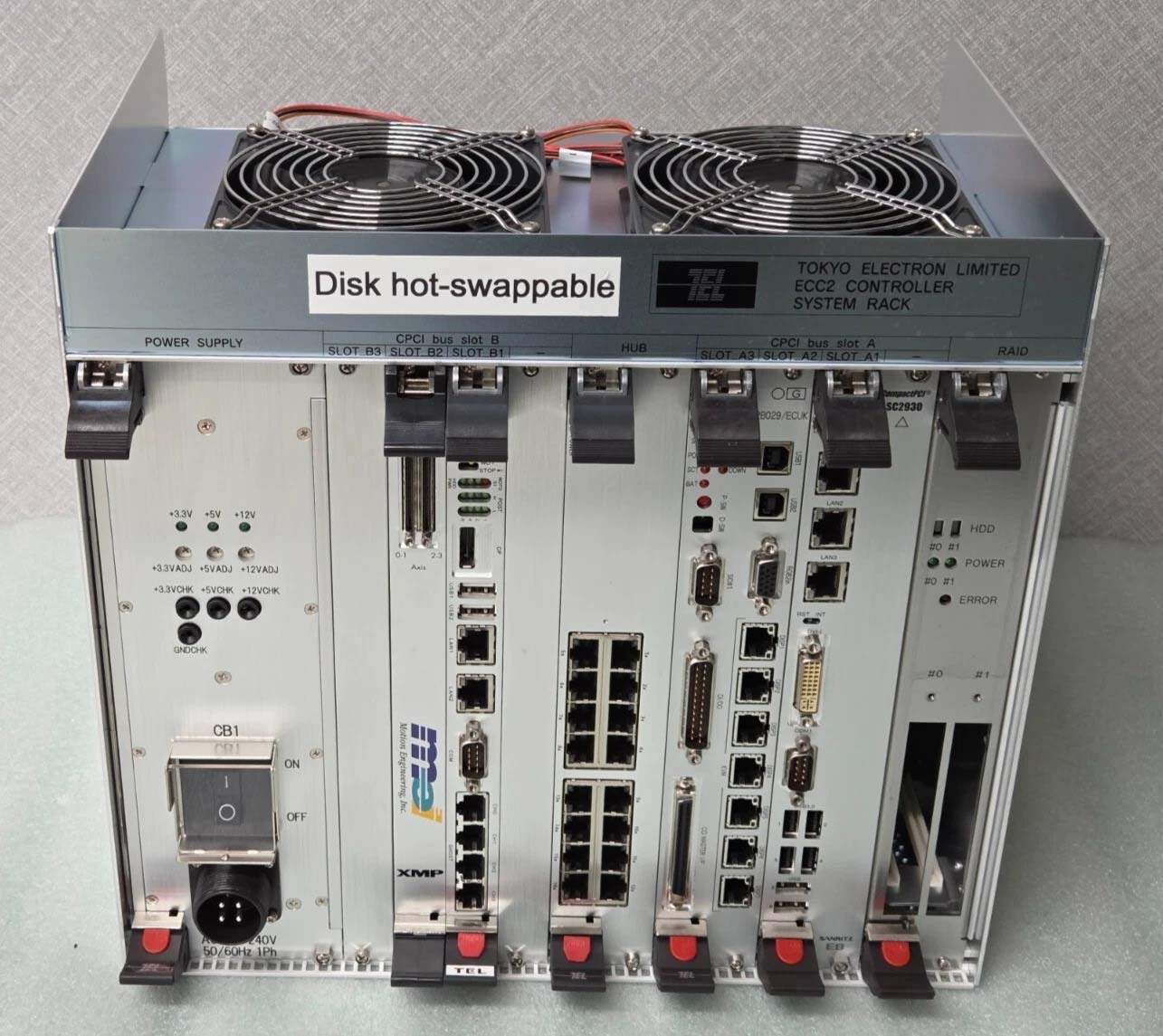

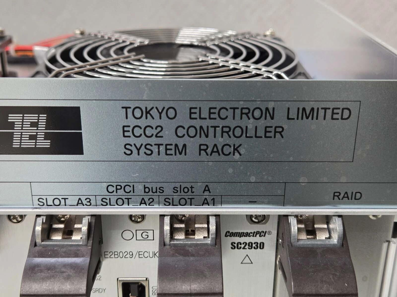
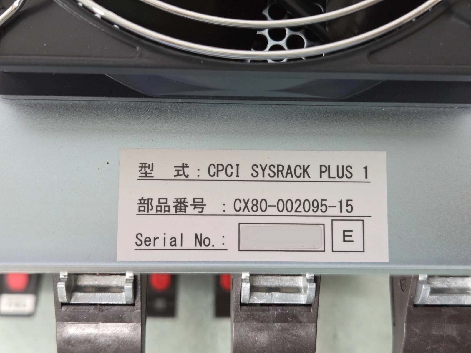
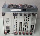
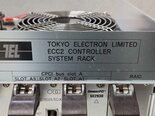
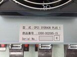
TEL / TOKYO ELECTRON ECC2 is a cutting-edge photoresist equipment that offers advanced technology and capabilities for the semiconductor manufacturing industry. This system is designed to meet the demanding requirements of producing high-quality semiconductor devices with precision and efficiency. TEL ECC2 unit is developed by TEL Limited (TOKYO ELECTRON), a leading provider of semiconductor equipment and solutions. At the core of TOKYO ELECTRON ECC2 machine is its photoresist processing capability, which plays a crucial role in the lithography process of semiconductor manufacturing. Photoresist is a light-sensitive material that is applied to a semiconductor wafer to transfer a pattern onto the surface during the photolithography process. ECC2 tool is equipped with advanced features to ensure accurate and uniform application of photoresist, resulting in high-resolution patterns and precise semiconductor device structures. One of the key features of TEL / TOKYO ELECTRON ECC2 asset is its high throughput capabilities, which enable rapid processing of semiconductor wafers without compromising on quality. The model is designed to handle large volumes of wafers efficiently, making it ideal for high-volume semiconductor manufacturing facilities. This high throughput is achieved through automated processes, advanced robotics, and optimized workflows that streamline the production process. TEL ECC2 equipment also offers superior process control and monitoring capabilities, allowing operators to maintain tight control over the photoresist deposition process. Advanced sensors and monitoring systems provide real-time feedback on key process parameters such as temperature, pressure, and flow rates, ensuring consistent and reliable performance. This level of process control is essential for achieving high yields and minimizing defects in semiconductor production. In addition to its high throughput and process control capabilities, TOKYO ELECTRON ECC2 system is designed for flexibility and customization to meet the varying requirements of different semiconductor manufacturing processes. The unit can be configured with a range of options and modules to support different photoresist types, wafer sizes, and process conditions. This flexibility allows semiconductor manufacturers to tailor the machine to their specific needs and optimize production for different device types and applications. Furthermore, ECC2 tool incorporates advanced automation and software capabilities to enhance efficiency and productivity in semiconductor manufacturing. Automated wafer handling, recipe management, and data analytics features streamline operations and reduce manual intervention, resulting in higher throughput and lower production costs. The asset also integrates with advanced manufacturing execution systems (MES) to enable seamless data transfer and process integration across the semiconductor production line. Overall, TEL / TOKYO ELECTRON ECC2 photoresist model represents a state-of-the-art solution for semiconductor manufacturers looking to achieve high-performance lithography processes with precision and efficiency. With its advanced technology, high throughput capabilities, superior process control, and flexibility, TEL ECC2 equipment is well-suited for demanding semiconductor production environments where quality, speed, and reliability are paramount.
There are no reviews yet