Used TEL / TOKYO ELECTRON ECC2 #293805091 for sale
URL successfully copied!

Tap to zoom
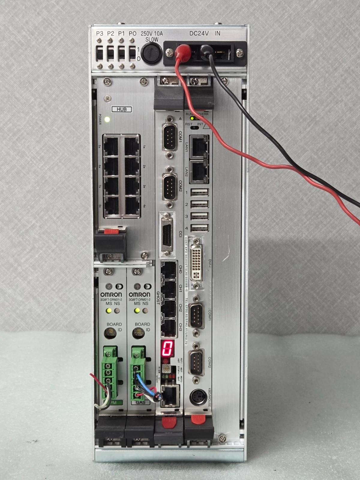

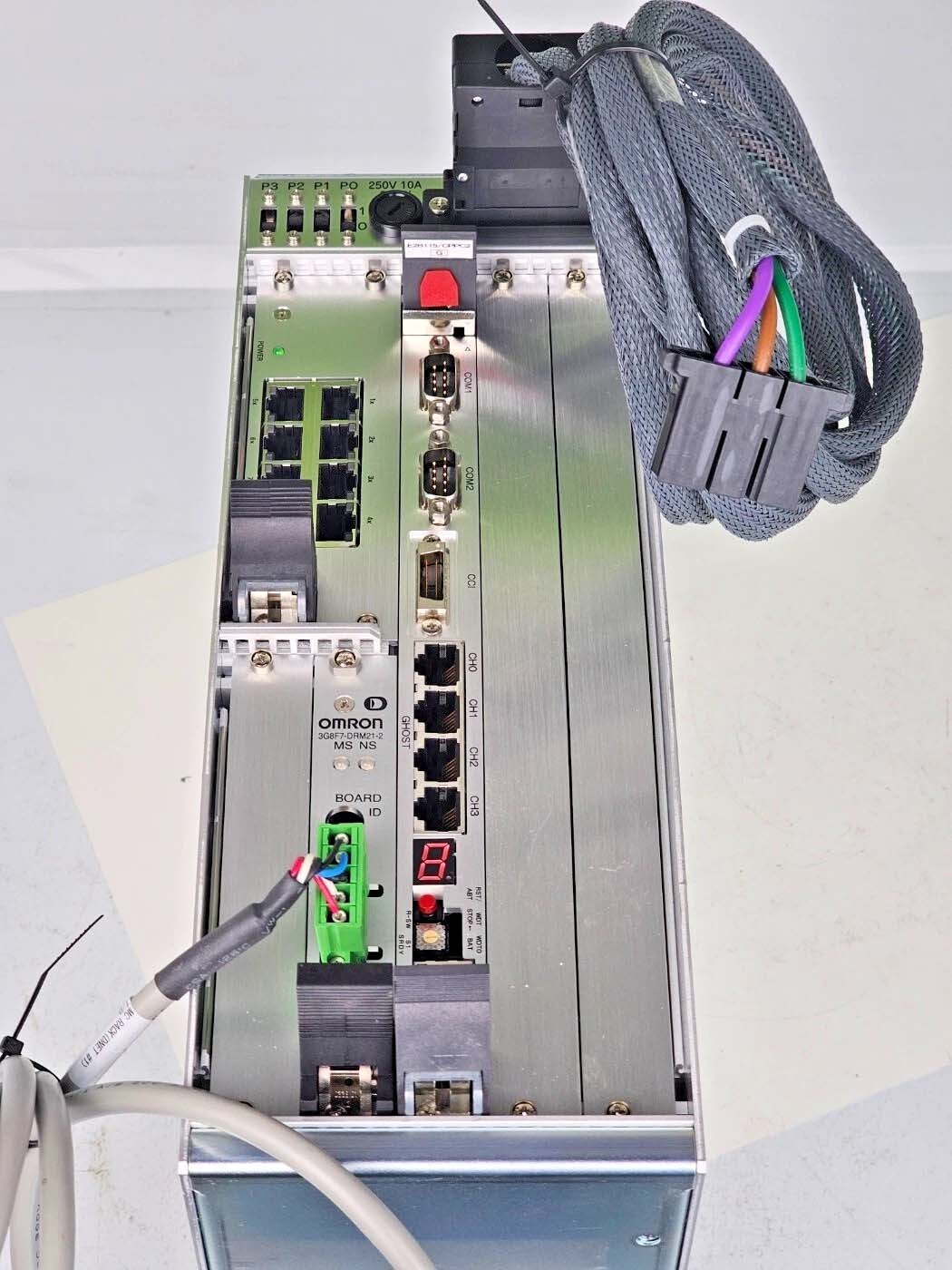
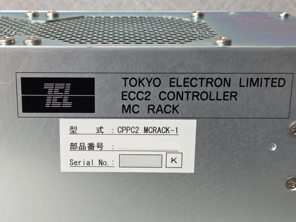
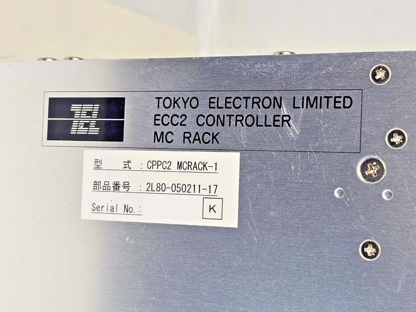
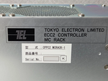
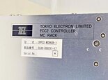
TEL / TOKYO ELECTRON ECC2 is an advanced photoresist equipment utilized in the semiconductor manufacturing industry for high-precision photolithography processes. As a crucial step in the fabrication of integrated circuits (ICs) and other electronic components, photolithography involves the transfer of circuit patterns onto silicon wafers using photoresist materials. TEL ECC2 system, developed by TEL Limited (TOKYO ELECTRON), offers a comprehensive solution for achieving superior patterning results with high accuracy and productivity. Functioning as a critical component of the photolithography process, TOKYO ELECTRON ECC2 photoresist unit demonstrates exceptional capabilities for patterning submicron features with minimal defects and high throughput. Leveraging cutting-edge technologies and innovative engineering, this machine enables semiconductor manufacturers to achieve advanced node scaling and improve the performance of next-generation ICs. One of the key features of ECC2 tool is its precise control over exposure, development, and etching processes during photolithography. By integrating sophisticated optics and advanced light sources, the asset ensures accurate pattern transfer onto the wafer surface with high resolution. TEL / TOKYO ELECTRON ECC2 model also incorporates advanced imaging algorithms and intelligent software algorithms to optimize exposure parameters and enhance image fidelity. In addition to its imaging capabilities, TEL ECC2 photoresist equipment offers exceptional uniformity and consistency in coating, developing, and etching processes. Through the use of advanced dispensing and spin-coating technologies, the system achieves uniform distribution of photoresist materials on the wafer surface, minimizing variations in film thickness and improving pattern fidelity. The precise control over development and etching parameters further enhances pattern quality and reduces defects in the final product. Furthermore, TOKYO ELECTRON ECC2 unit is designed for high productivity and operational efficiency in semiconductor manufacturing facilities. With features such as automated wafer handling, real-time monitoring, and remote diagnostics, the machine streamlines production workflows and minimizes downtime. ECC2 tool also offers advanced process control capabilities, enabling manufacturers to achieve tight process windows and consistent results across multiple production runs. Another important aspect of TEL / TOKYO ELECTRON ECC2 photoresist asset is its compatibility with a wide range of photoresist materials and semiconductor processes. Whether used for positive or negative tone photoresists, the model can accommodate various chemistries and formulations to meet specific device requirements. This flexibility ensures that manufacturers have the versatility to adapt to changing process demands and technology nodes. Overall, TEL ECC2 equipment represents a state-of-the-art solution for advanced photolithography applications in semiconductor manufacturing. By delivering superior patterning performance, exceptional process control, and high productivity, the system empowers manufacturers to achieve optimal results in the production of cutting-edge semiconductor devices. With its innovative design, advanced features, and reliability, TOKYO ELECTRON ECC2 unit is a key enabler for driving technological advancements and innovation in the semiconductor industry.
There are no reviews yet