Used TEL / TOKYO ELECTRON ECC2 #293808145 for sale
URL successfully copied!
Tap to zoom
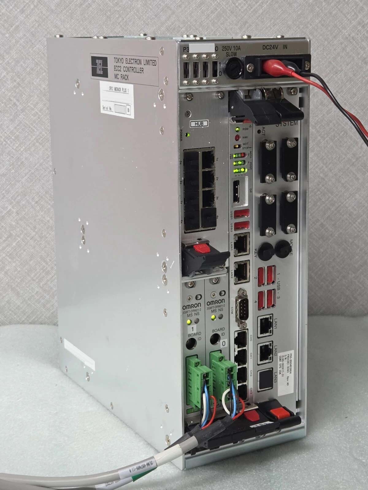

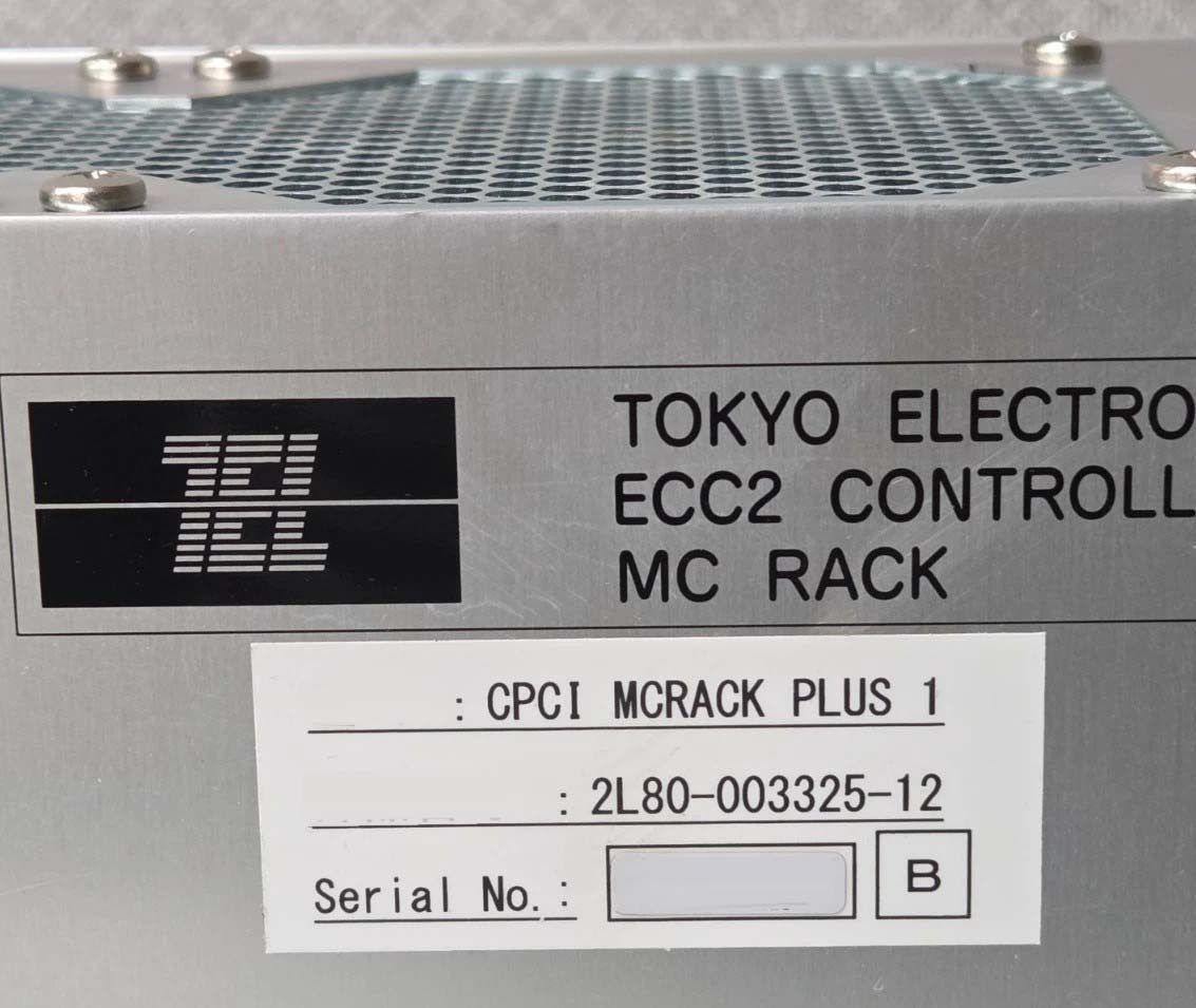
TEL (TEL / TOKYO ELECTRON ECC2) is a cutting-edge photoresist processing equipment utilized in the semiconductor industry for photolithography processes. Photolithography is a fundamental technique used to transfer patterns onto semiconductor wafers, playing a crucial role in the manufacturing of integrated circuits. TEL ECC2 system is designed by TOKYO ELECTRON, a leading supplier of semiconductor manufacturing equipment. The unit incorporates advanced technologies to achieve precise and efficient photoresist processing, ensuring high accuracy and repeatability in pattern transfer. The acronym TOKYO ELECTRON ECC2 stands for 'Electronically Controlled Coater Cluster,' emphasizing the machine's electronic control capabilities for coating photoresist materials. At the core of ECC2 tool is the photoresist processing module, which consists of several key components. The asset features a coater cluster unit responsible for applying a uniform layer of photoresist material onto the semiconductor substrate. This process is critical to ensure the accurate replication of patterns during subsequent steps in the semiconductor manufacturing process. One of the key strengths of TEL / TOKYO ELECTRON ECC2 model is its electronic control capabilities, which enable precise adjustment of coating parameters such as spin speed, dispense volume, and spin time. This level of control ensures uniformity in the thickness of the photoresist layer, leading to consistent patterning results across the semiconductor wafer. Furthermore, TEL ECC2 equipment integrates advanced monitoring and feedback mechanisms to optimize coating performance. In-line metrology tools are utilized to measure the thickness and uniformity of the photoresist layer in real-time, providing valuable data for process control and optimization. By continuously monitoring and adjusting coating parameters, the system can achieve high levels of accuracy and reproducibility in pattern transfer. In addition to its coating capabilities, TOKYO ELECTRON ECC2 unit also incorporates a range of features to enhance productivity and efficiency in photoresist processing. The machine is designed for high-throughput operations, allowing semiconductor manufacturers to achieve rapid processing speeds without compromising on quality. By automating key processes and minimizing manual interventions, ECC2 tool streamlines photoresist processing workflows and reduces the risk of human errors. Another notable feature of TEL / TOKYO ELECTRON ECC2 asset is its compatibility with a wide range of photoresist materials commonly used in semiconductor manufacturing. The model can accommodate different types of photoresists with varying viscosities, enabling semiconductor manufacturers to adapt to diverse process requirements and technology nodes. This flexibility makes TEL ECC2 equipment a versatile solution for a variety of applications in the semiconductor industry. Overall, TOKYO ELECTRON ECC2 system represents a state-of-the-art solution for photoresist processing in semiconductor manufacturing. With its electronic control capabilities, advanced monitoring tools, high-throughput design, and compatibility with diverse photoresist materials, ECC2 unit offers semiconductor manufacturers a reliable and efficient platform for achieving precise patterning results in the fabrication of advanced integrated circuits.
There are no reviews yet