Used TEL / TOKYO ELECTRON ECC2 #293808146 for sale
URL successfully copied!
Tap to zoom
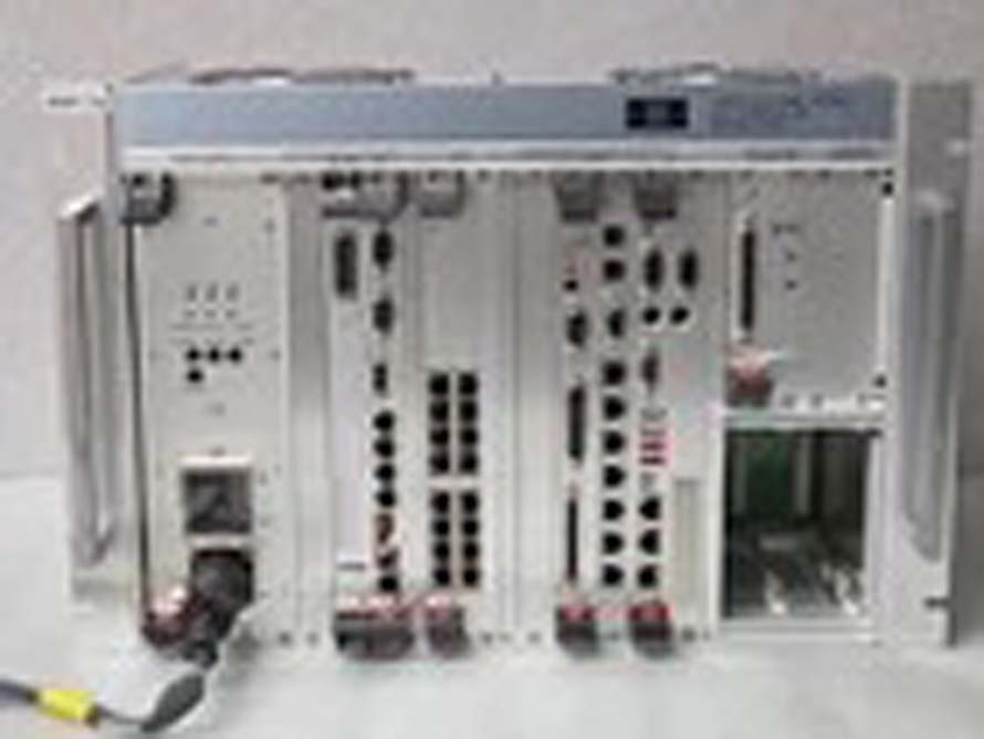

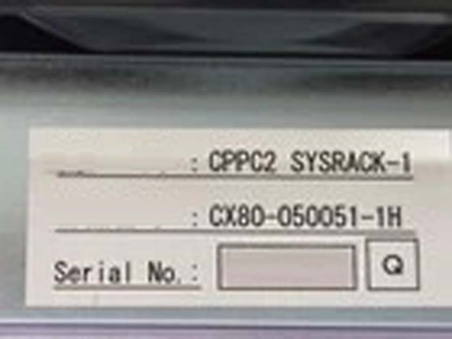
TEL / TOKYO ELECTRON ECC2 is a state-of-the-art photoresist equipment that is specifically designed for advanced semiconductor manufacturing processes. This system plays a crucial role in the production of integrated circuits by enabling high precision patterning of photoresist materials on silicon wafers. TEL ECC2 unit incorporates cutting-edge technology and features to meet the demanding requirements of leading semiconductor manufacturers. At the heart of TOKYO ELECTRON ECC2 machine is its advanced exposure mechanism, which utilizes extremely high precision optical alignment and projection techniques to define the intricate patterns required for semiconductor devices. The tool utilizes a complex series of lenses, mirrors, and masks to project the desired pattern onto the photoresist-coated wafer with incredible accuracy down to sub-nanometer levels. This level of precision is essential for creating smaller transistor features and increasing the density of components on the silicon wafer, which ultimately leads to improved performance and functionality of the integrated circuits. ECC2 asset also features a sophisticated stage control model that allows for precise movement and positioning of the wafer during the exposure process. This stage control equipment ensures that the wafer is held in the correct position and orientation throughout the exposure, guaranteeing that the pattern is accurately transferred onto the photoresist layer. Additionally, TEL / TOKYO ELECTRON ECC2 system incorporates advanced algorithms for real-time monitoring and adjustment of the stage position to compensate for any minute variations or disturbances that may occur during the exposure process. One of the key advantages of TEL ECC2 unit is its high throughput capabilities, which are essential for meeting the high-volume production requirements of modern semiconductor manufacturing facilities. The machine is designed to process wafers at a rapid pace while maintaining superior pattern fidelity and consistency across the entire wafer surface. This high throughput is achieved through a combination of advanced exposure techniques, optimized stage movements, and efficient wafer handling processes that minimize downtime and maximize productivity. Furthermore, TOKYO ELECTRON ECC2 tool is equipped with advanced process control and automation features that ensure the reproducibility and consistency of patterning results across multiple wafers and production runs. The asset can automatically calibrate and adjust various parameters such as exposure dose, focus, and alignment settings to compensate for variations in photoresist properties, wafer topography, and environmental conditions. This level of automation reduces the risk of human error and enhances the overall yield and quality of the semiconductor devices manufactured using ECC2 model. In conclusion, TEL / TOKYO ELECTRON ECC2 photoresist equipment represents a cutting-edge solution for high-precision patterning in semiconductor manufacturing. With its advanced exposure mechanism, sophisticated stage control system, high throughput capabilities, and automation features, TEL ECC2 unit enables semiconductor manufacturers to achieve superior patterning results with unmatched accuracy and efficiency. By leveraging the capabilities of TOKYO ELECTRON ECC2 machine, semiconductor manufacturers can advance their technology roadmap and deliver next-generation semiconductor devices that push the boundaries of performance and miniaturization.
There are no reviews yet