Used TEL / TOKYO ELECTRON ECC2 #293808147 for sale
URL successfully copied!

Tap to zoom
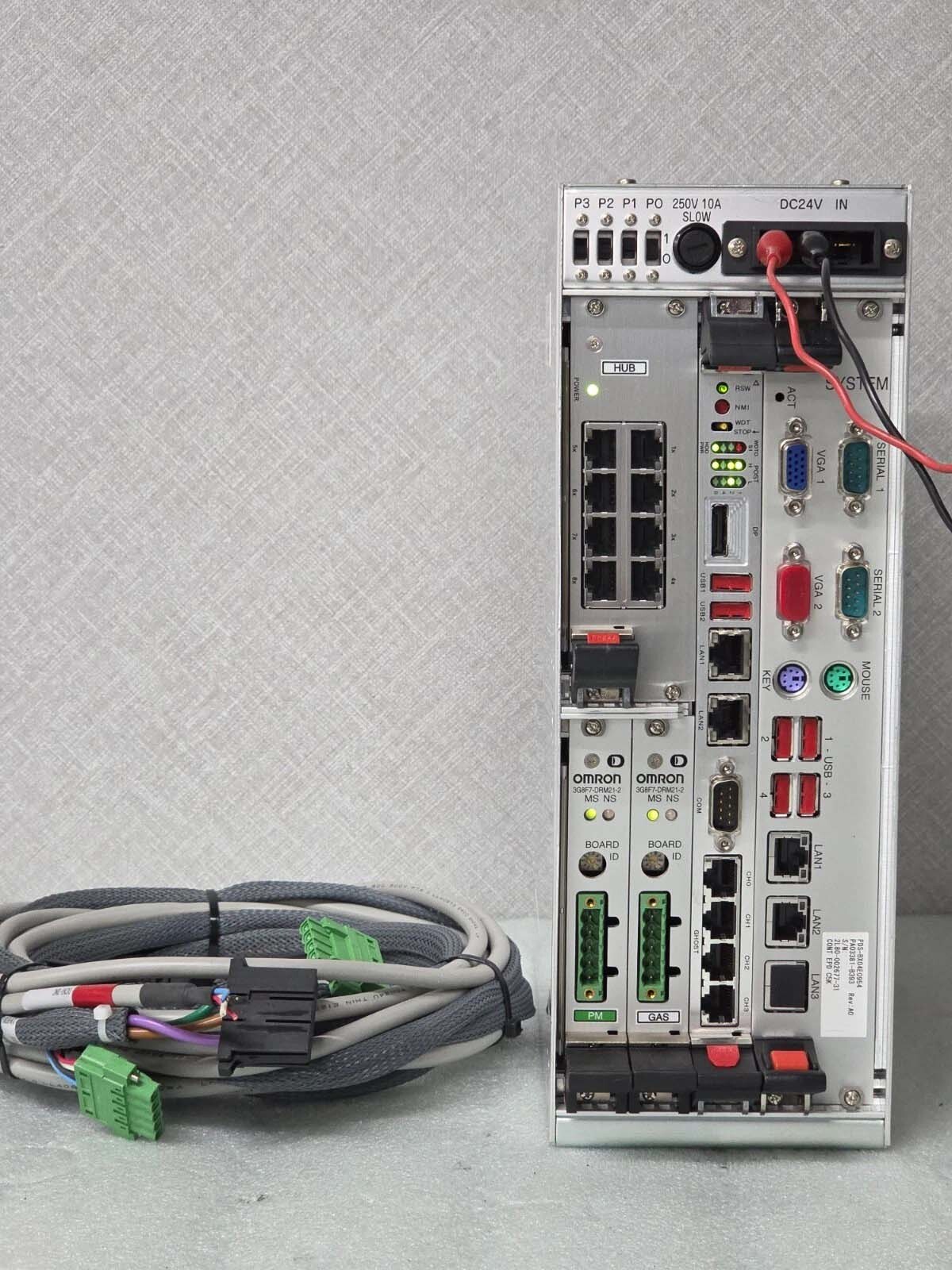

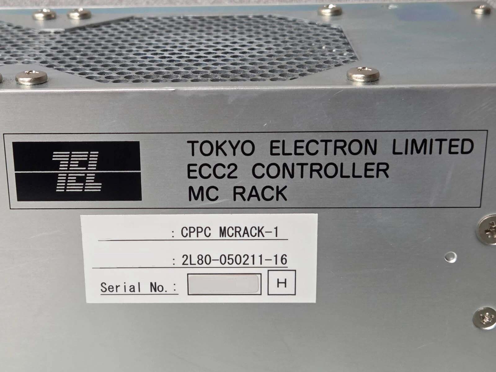
TEL (TOKYO ELECTRON Limited) is a prominent manufacturer of semiconductor and flat panel display production equipment, among which TEL / TOKYO ELECTRON ECC2 model is a sophisticated photoresist equipment utilized in the semiconductor manufacturing process. TEL ECC2 system plays a critical role in the photolithography process, which is an essential step in semiconductor fabrication. TOKYO ELECTRON ECC2 unit is designed to deposit and pattern a light-sensitive material, known as photoresist, onto semiconductor wafers to define the circuit patterns on the integrated circuits. This process involves a series of steps, including coating the wafer with a thin layer of photoresist, exposing it to UV light through a mask that contains the circuit pattern, developing the exposed wafer to remove the unwanted photoresist, and finally etching the underlying layers to transfer the pattern onto the wafer. One of the key features of ECC2 machine is its precise and uniform coating capabilities, which are essential for achieving high-resolution patterns with tight tolerances. The tool utilizes advanced techniques such as spin coating or spray coating to ensure a uniform layer of photoresist is deposited on the wafer surface. Additionally, TEL / TOKYO ELECTRON ECC2 asset incorporates temperature and humidity controls to optimize the photoresist coating process and minimize variations in film thickness. In terms of exposure capabilities, TEL ECC2 model is equipped with a sophisticated mask alignment and exposure unit that enables accurate alignment of the mask pattern to the wafer surface. This ensures that the circuit patterns are precisely transferred onto the wafer with minimal alignment errors. The equipment also offers a variety of exposure modes, such as proximity, projection, or stepper modes, to cater to different lithography requirements. Furthermore, TOKYO ELECTRON ECC2 system features a robust development module that facilitates the removal of the exposed photoresist to reveal the underlying pattern on the wafer. The development process is carefully controlled to ensure that the photoresist is selectively removed from the exposed areas while preserving the unexposed regions. This step is crucial for defining the circuit features accurately and reliably. ECC2 unit is also equipped with advanced monitoring and control systems that allow real-time monitoring of key parameters such as temperature, pressure, and exposure dosage. These features enable the machine to maintain consistent and repeatable process conditions, leading to high-quality and reliable patterning results. Additionally, the tool offers comprehensive diagnostic tools and software interfaces for easy operation and troubleshooting. In conclusion, TEL / TOKYO ELECTRON ECC2 photoresist asset is a sophisticated and reliable tool for semiconductor manufacturing, specifically tailored for the critical photolithography process. With its precise coating capabilities, accurate exposure units, and robust development module, TEL ECC2 model enables semiconductor manufacturers to achieve high-resolution patterns with tight tolerances, ultimately contributing to the production of advanced integrated circuits with improved performance and functionality.
There are no reviews yet