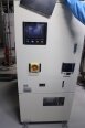
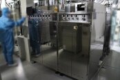
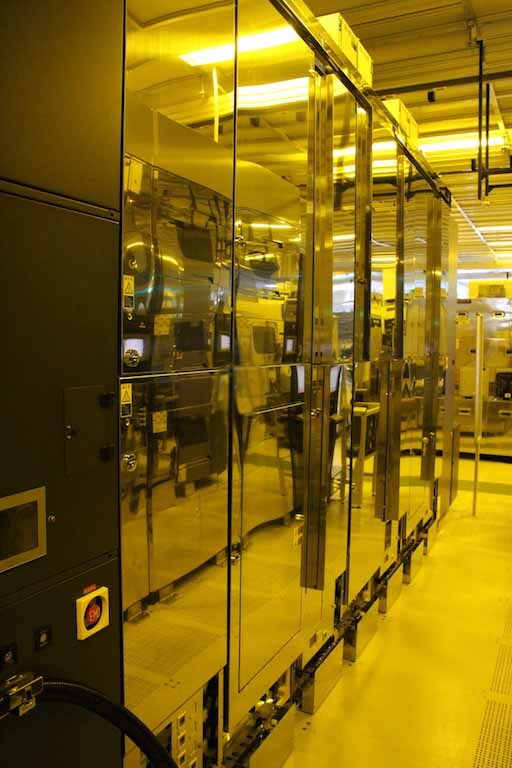
Used TEL / TOKYO ELECTRON Lithius i+ #9171607 for sale
URL successfully copied!
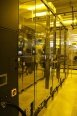
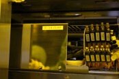
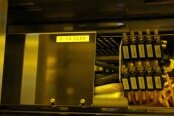
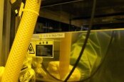
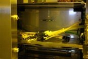
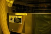
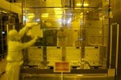
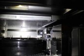
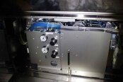
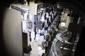
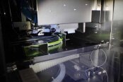
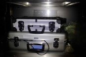
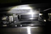
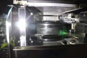
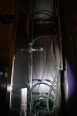
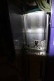
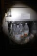
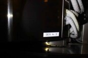
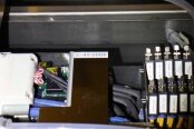
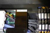
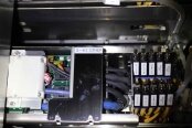
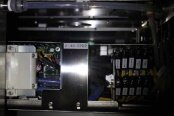
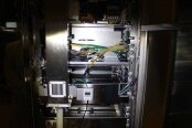

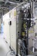
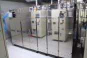
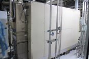
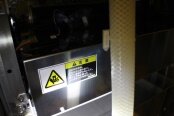
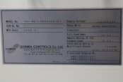
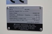
Tap to zoom

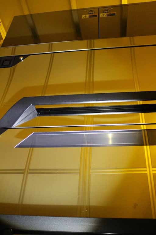
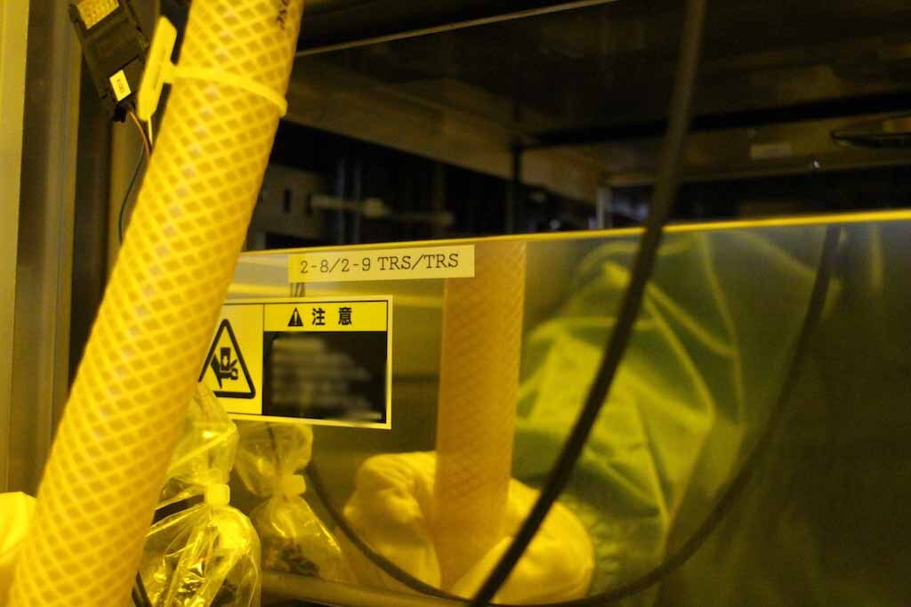
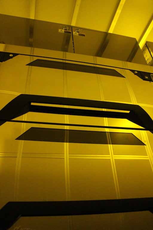
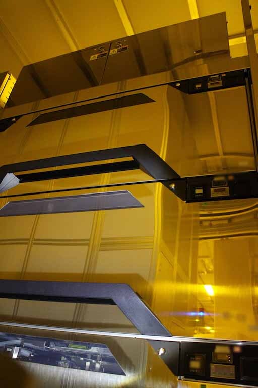
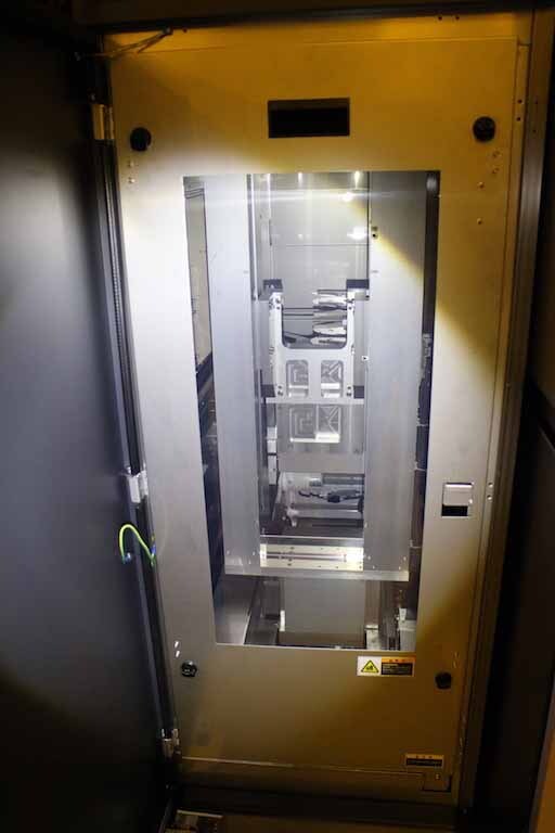
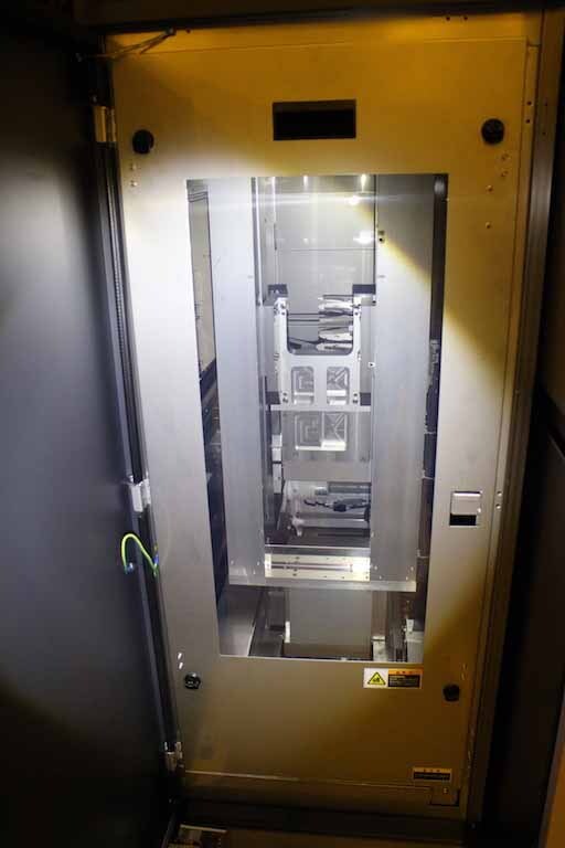
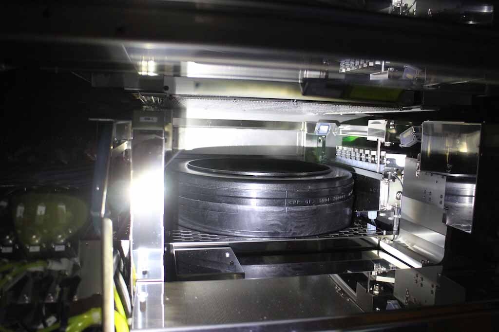
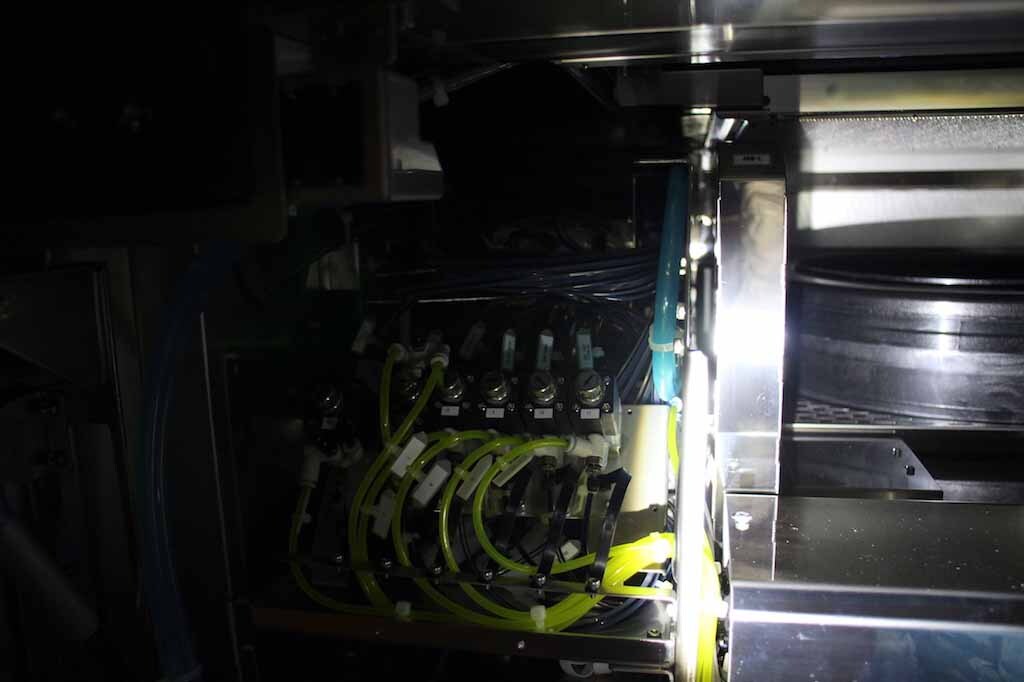
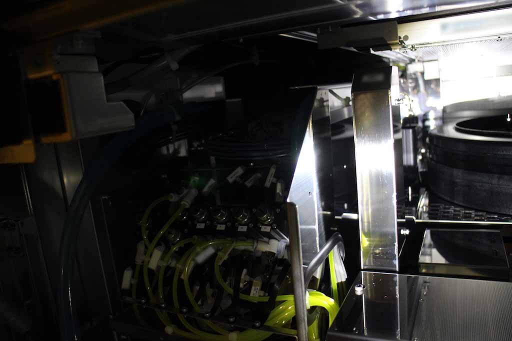
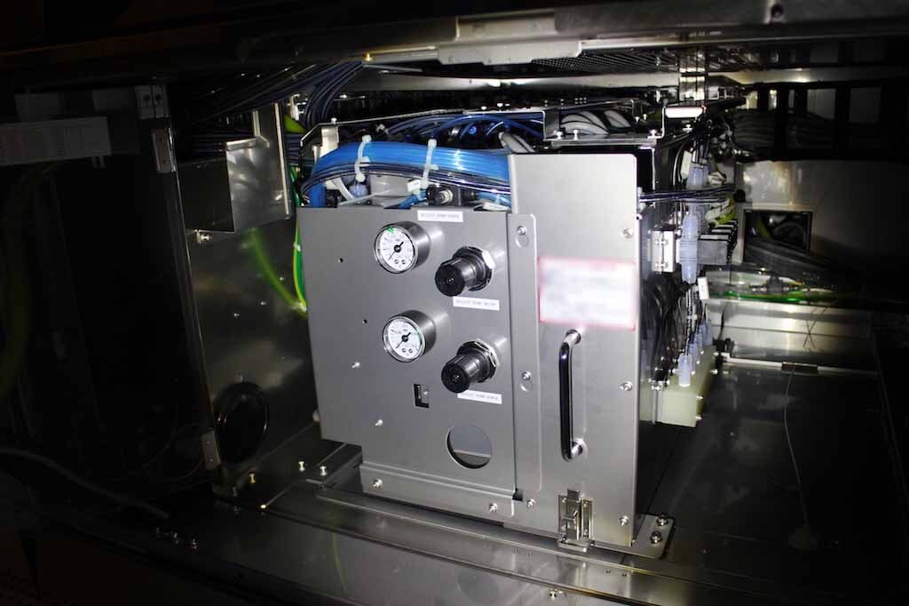
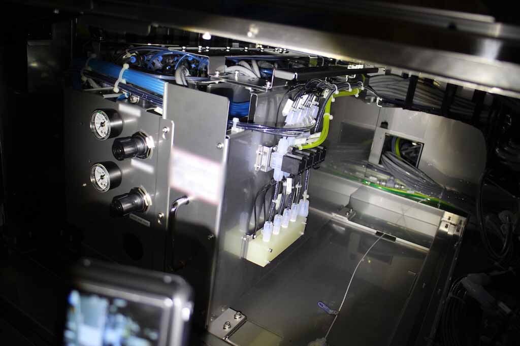
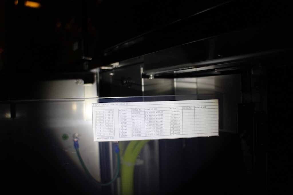
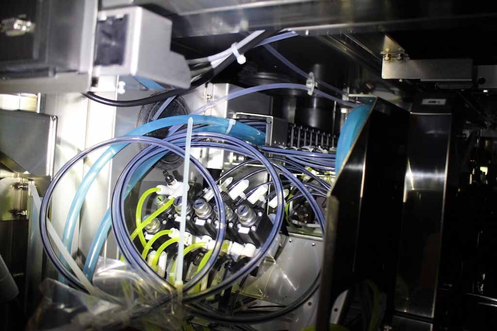
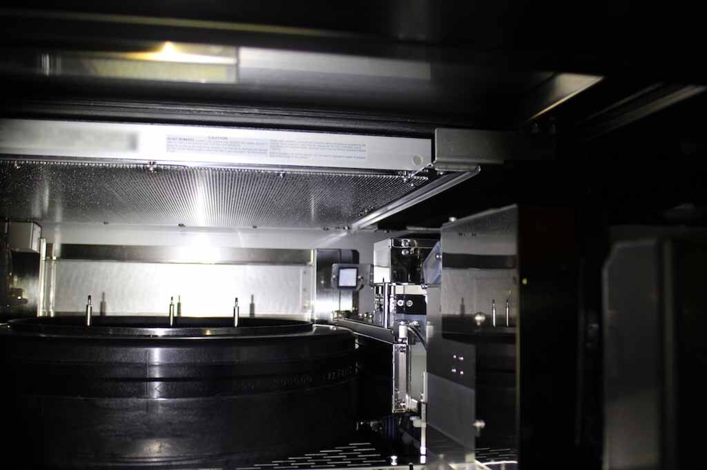
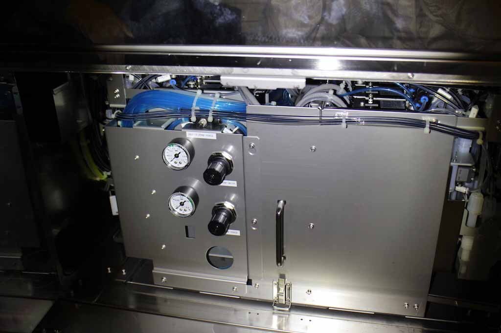
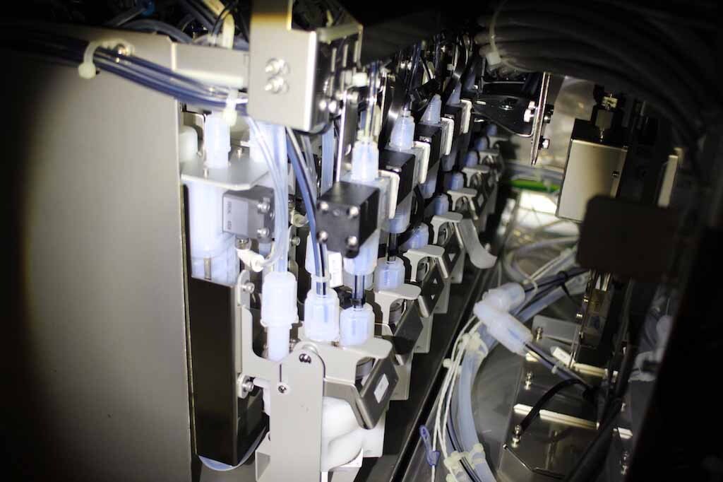
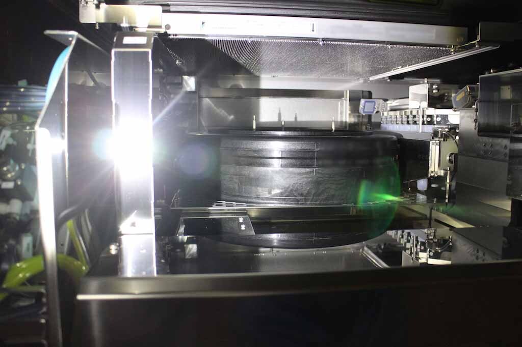
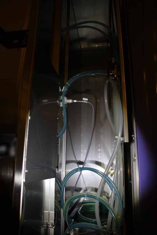
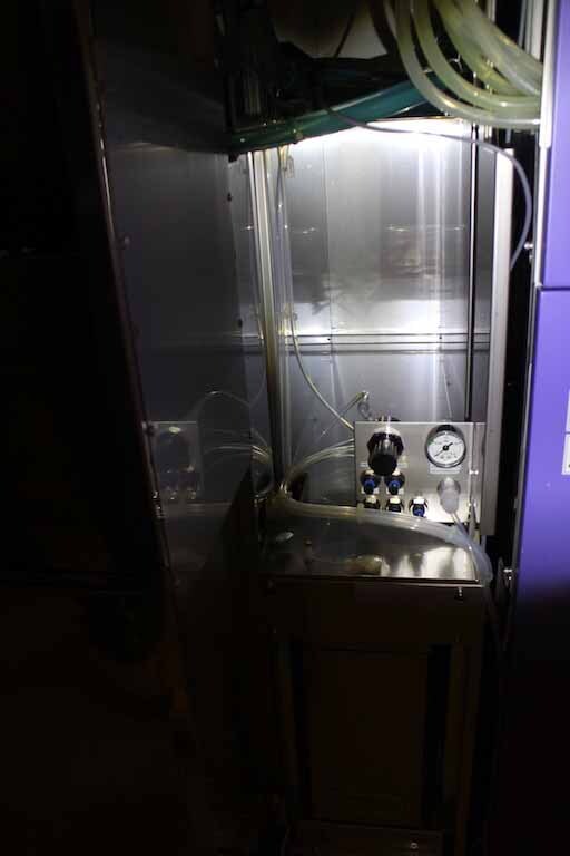
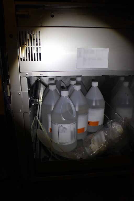
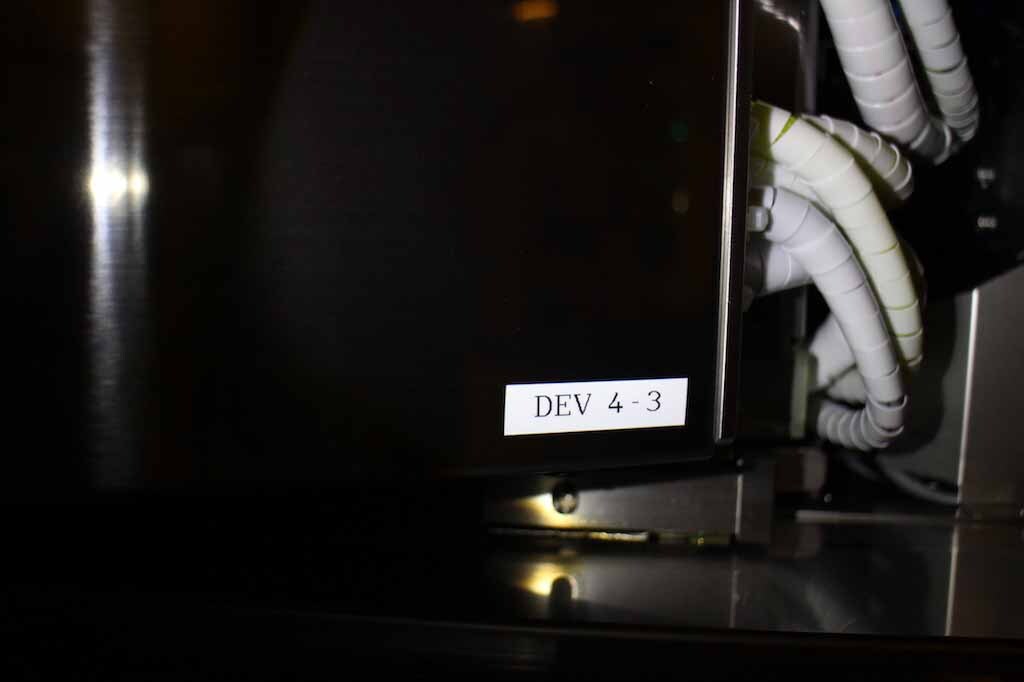
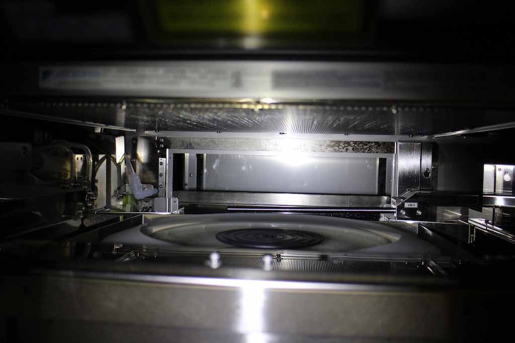
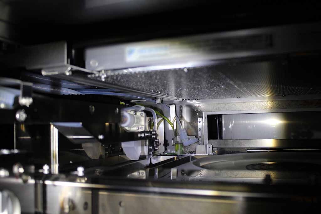
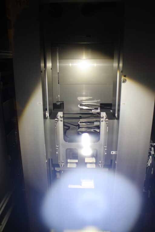
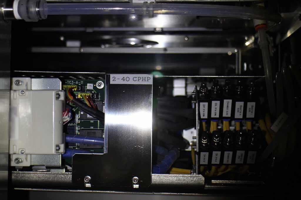
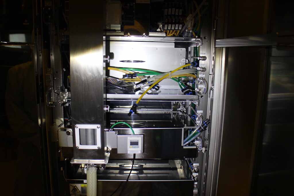
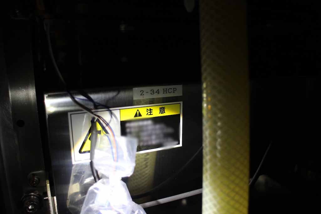
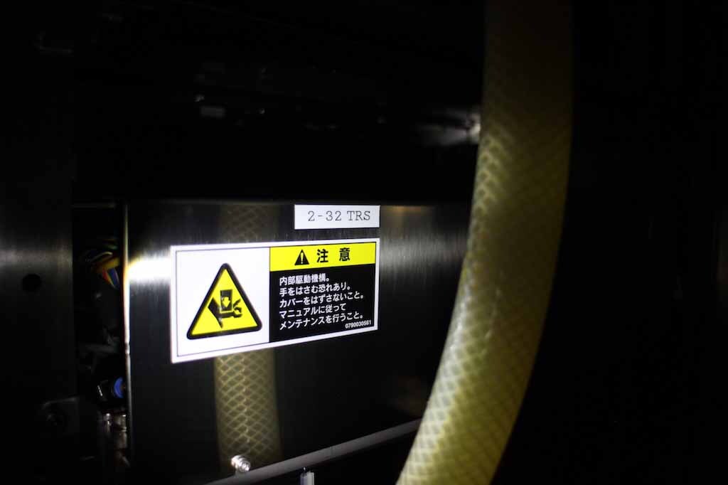
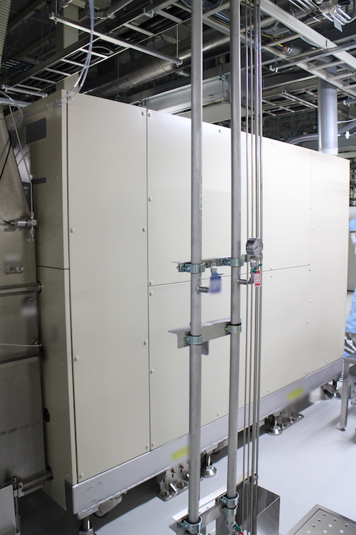
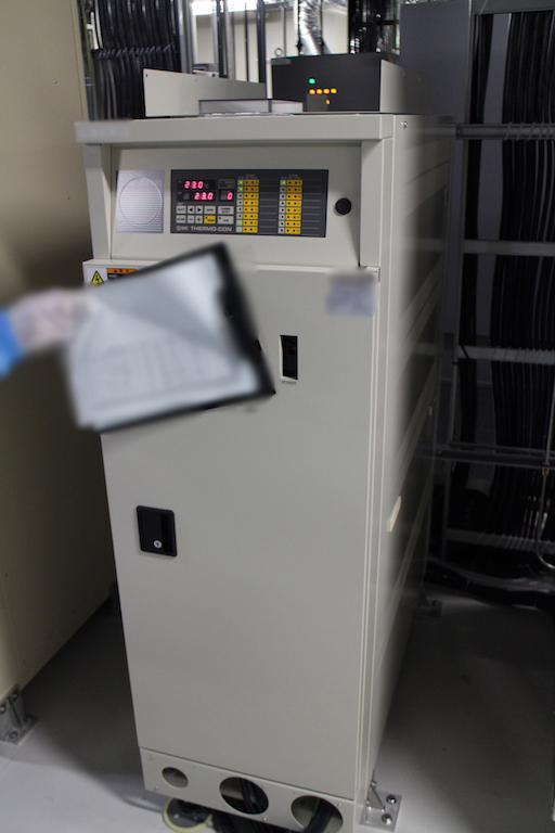
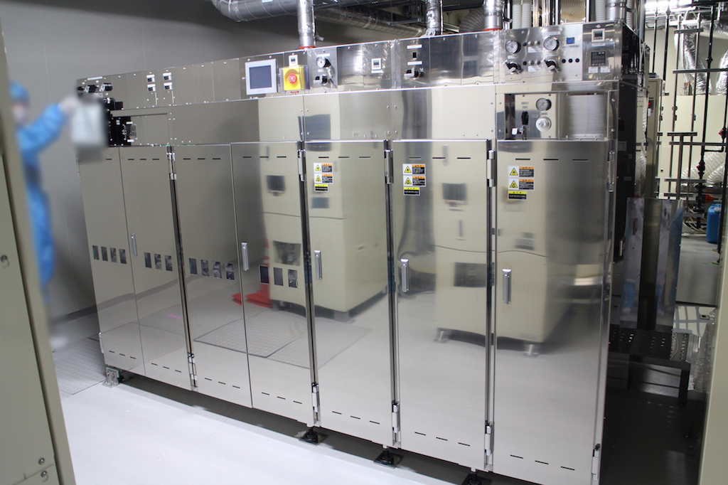
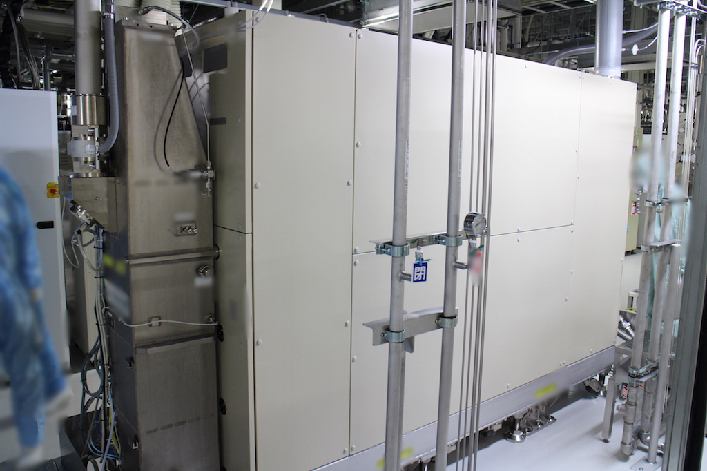
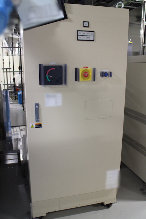
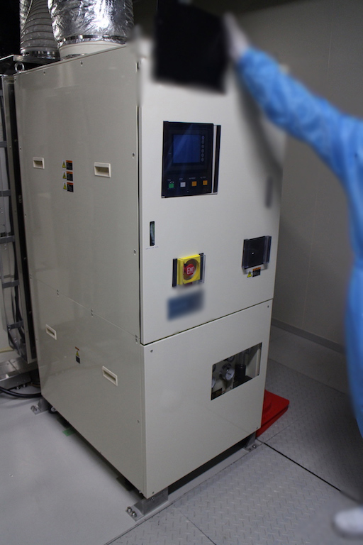
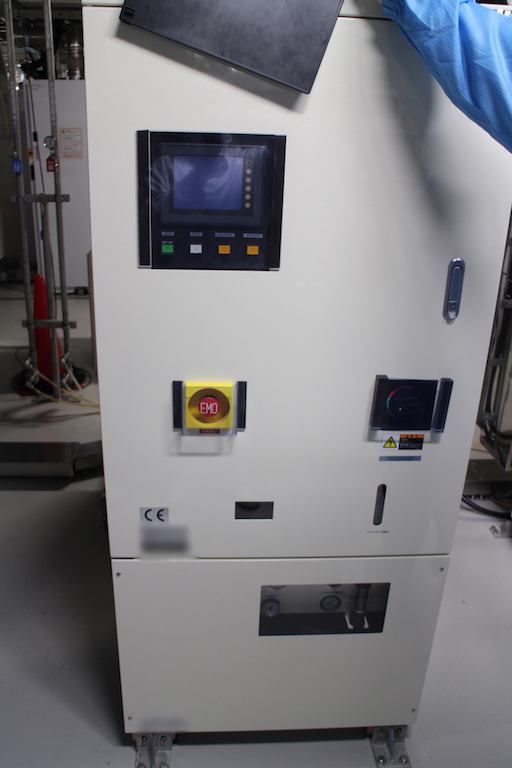
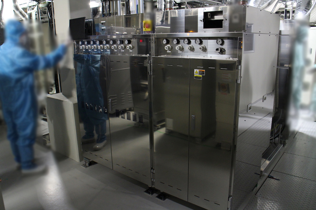
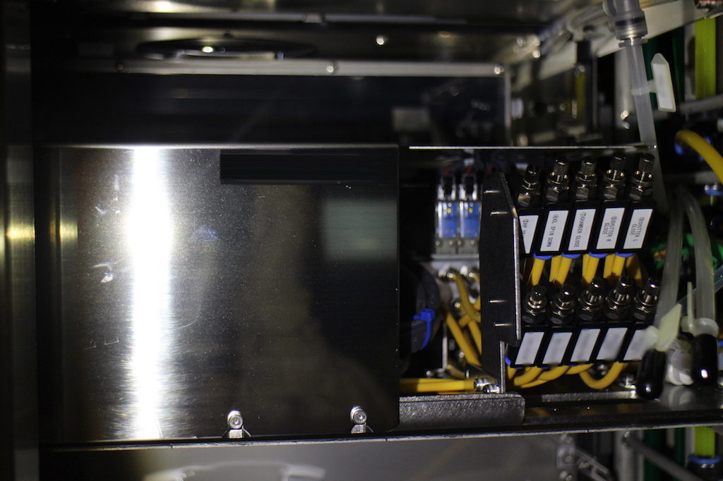
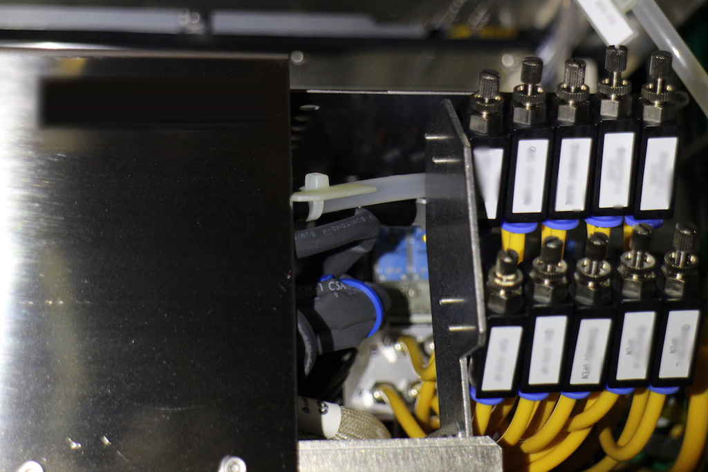
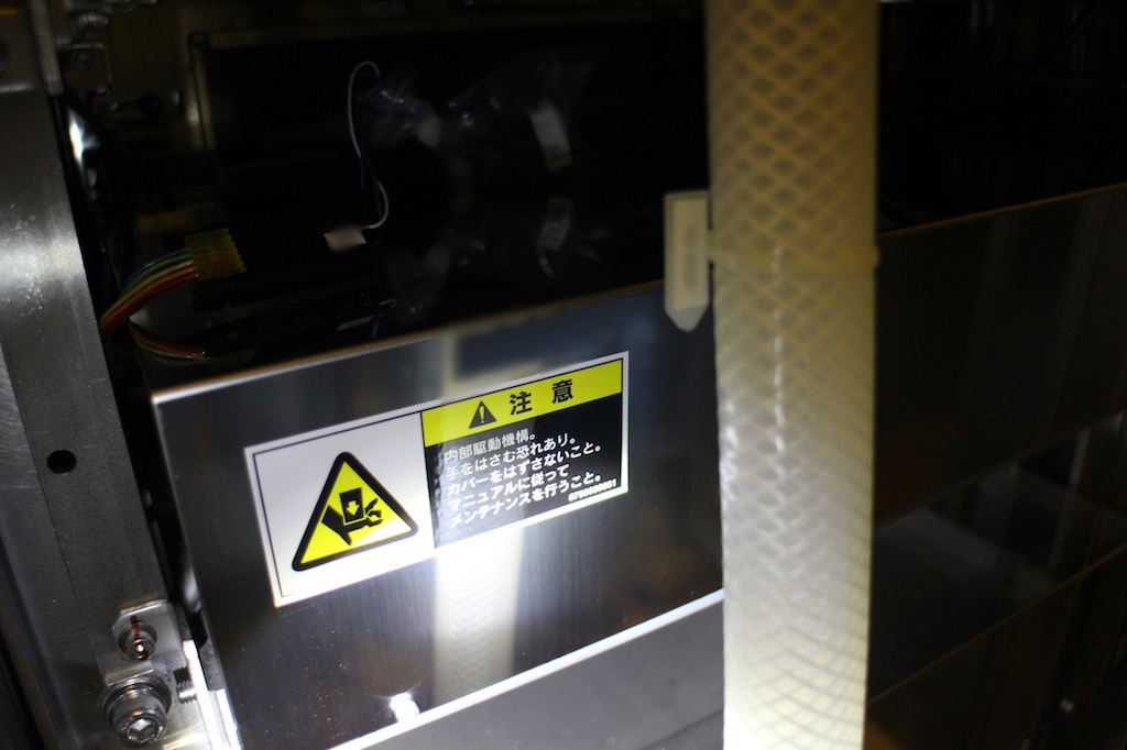
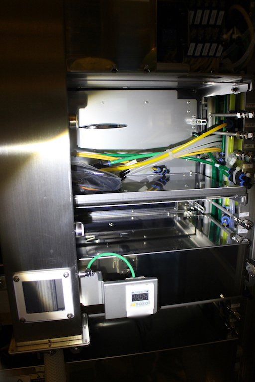
ID: 9171607
Wafer Size: 12"
Vintage: 2002
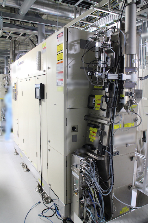
Coater / Developer system, 12"
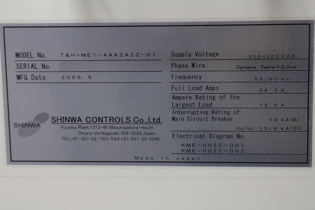
Model no: T&H-ME1-4AAZAZZ-01
Wafer type: Notch
Wafer material: Si
Signal tower: ETC (4) Lamps
On-line interface: SECS II / GEM
In-line: Yes
Make: NIKON
Model: NSR
Main controller: Version 4
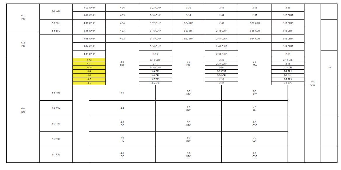
Layout type: IFB, PSB, CSB (Touch)
2002 vintage.
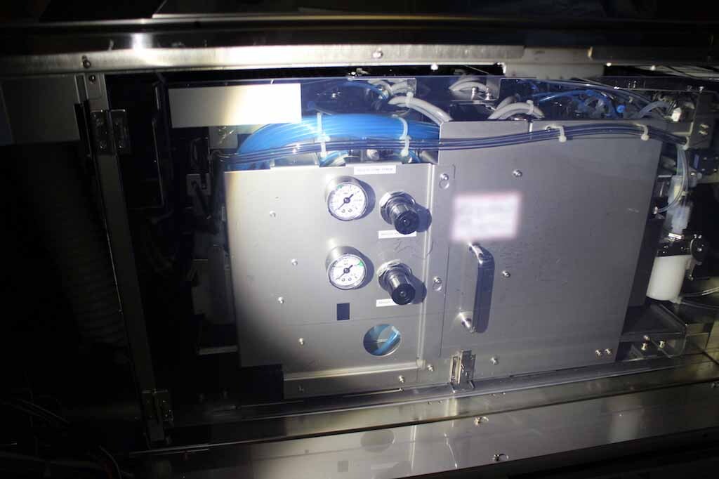
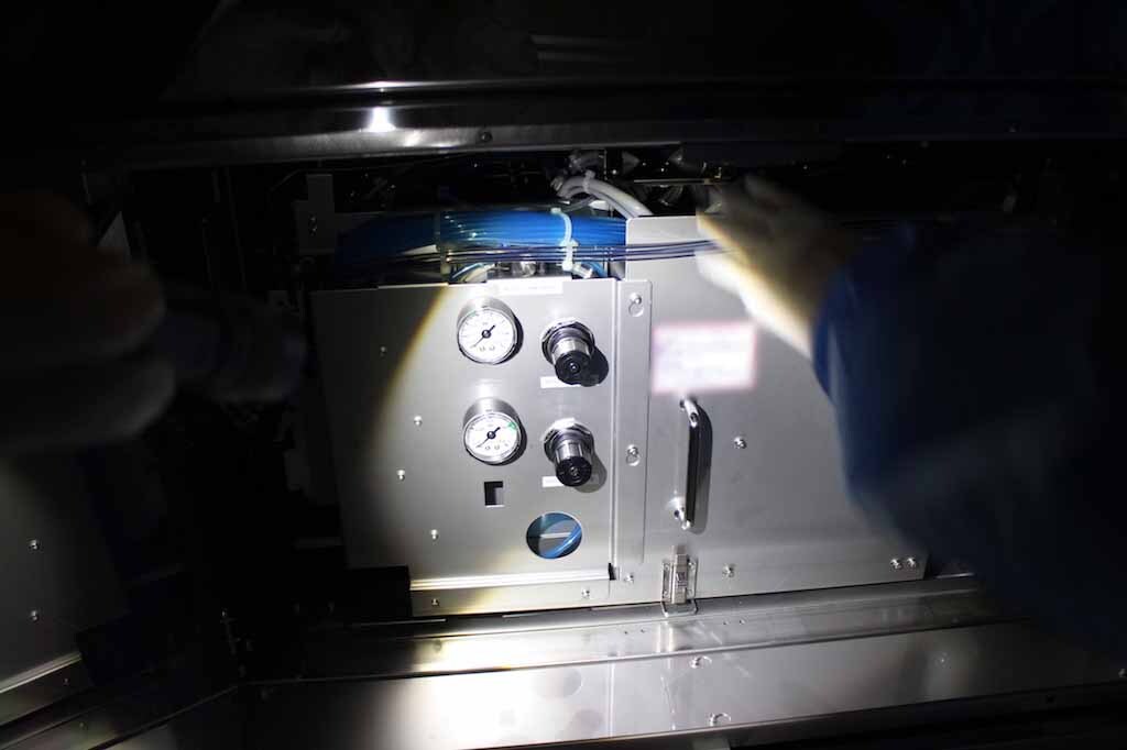
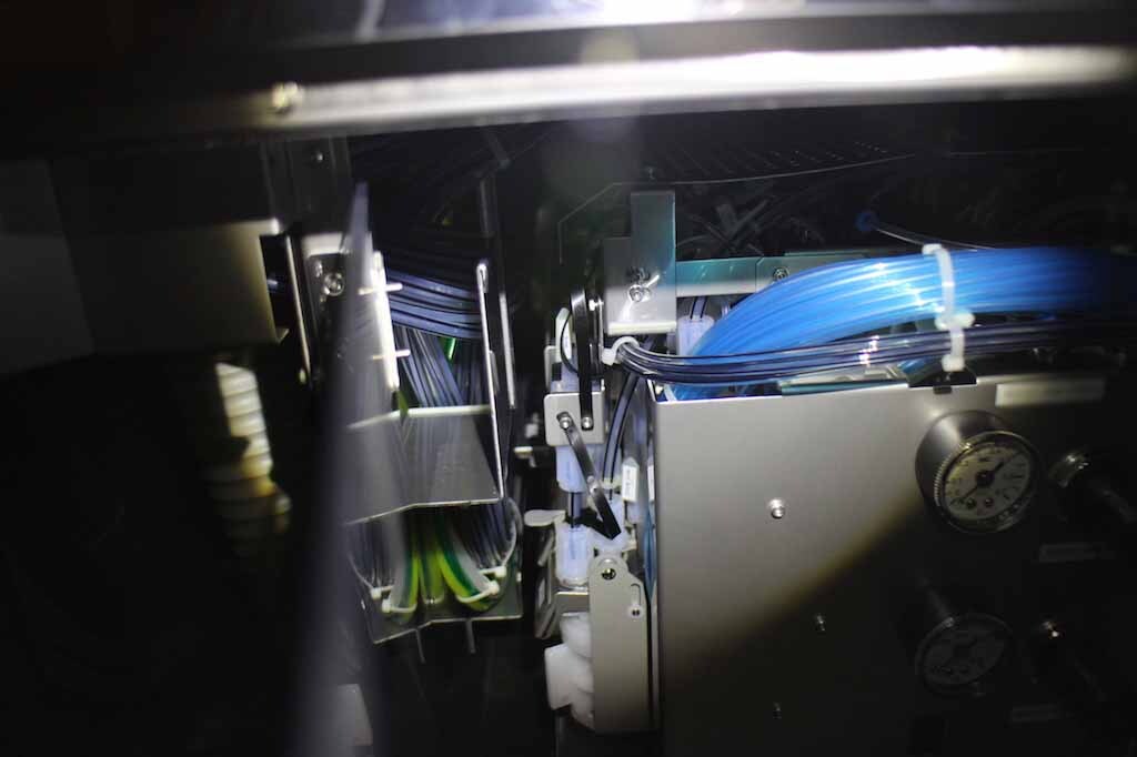
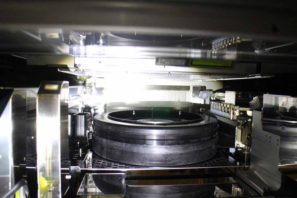
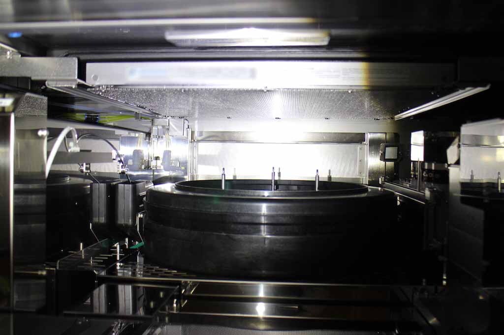
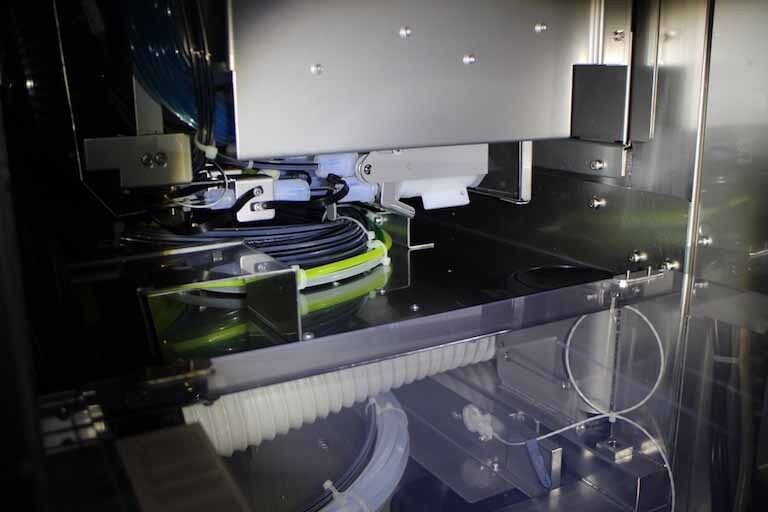
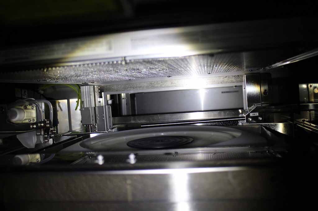
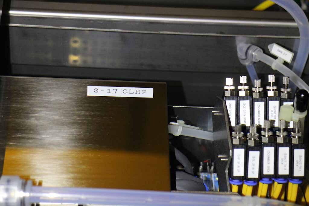
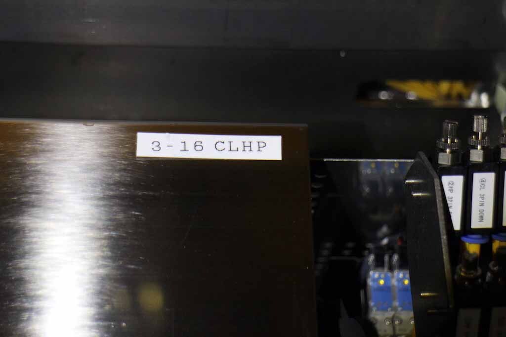
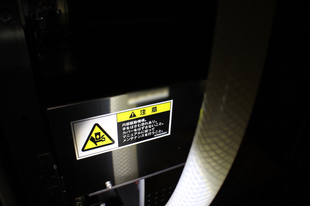
TEL / TOKYO ELECTRON Lithius i+ is a photoresist equipment designed to provide an accurate and efficient lithographical process in the microfabrication of semiconductor devices. It is designed to ensure the highest possible levels of accuracy and production in the manufacture of devices at millimetre and nanometre scale. The system is built around a litho cell which consists of a shutter, lens and exposure beam source, each with digital controls. The shutter is an advanced piezo actuator, controlled by a controller to ensure optimal positioning and exposure. The lens provides a high-resolution diffractive imaging optics for patterning on a wafer. The proximity of the lens to the wafer ensures a high-resolution geometry for the lithographical process. The exposure beam source is a laser which makes use of digital optics and optics models to provide the optimal pattern on the wafer surface. The unit has a focused, short pulse laser source which is used for creating high-resolution patterns, whether for microfabrication of wafers or for laser-direct written materials. This focused, short-pulse laser source is ideal for many applications, including modifications to existing features on a wafer, creation of new features, and a wide range of applications that require lithographical accuracy. The source is capable of projecting an image on a variety of materials without distortion or damage, providing a wide range of lithographical capabilities in an efficient manner. The machine also includes a number of other components which enable efficient production capability. These components include automatic substrate cassette handling, as well as an easily programmable auto-focus capability. The auto focus ensures that each wafer is exposed and patterned with optimal accuracy. The control platform is a sophisticated user interface which is designed to be highly intuitive and user-friendly, making the tool capable of many complex tasks, including multiple exposures, development of multiple recipes, and counting of components. The asset also includes a variety of traceability capabilities, including post-exposure alignment, tracking, and high speed wafer warpage correction. This makes it possible to use the model with even the most demanding production schedules. TEL Lithius i+ is an advanced photoresist equipment that provides efficient lithographical solutions with unmatched accuracy. The range of components, automated features and traceability options ensures that the system can be used for a broad variety of applications and production requirements.
There are no reviews yet