Used TEL / TOKYO ELECTRON Lithius #293671305 for sale
URL successfully copied!
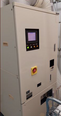

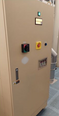

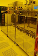
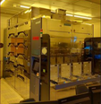

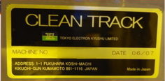


Tap to zoom
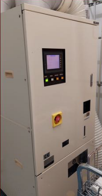

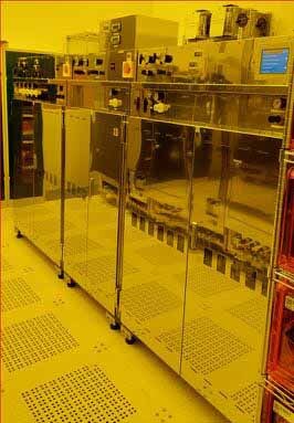
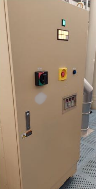
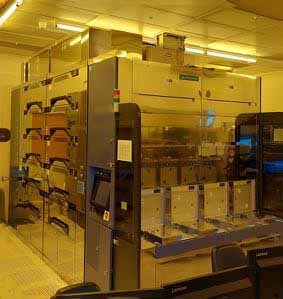
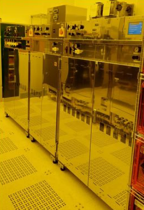
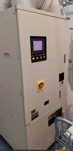
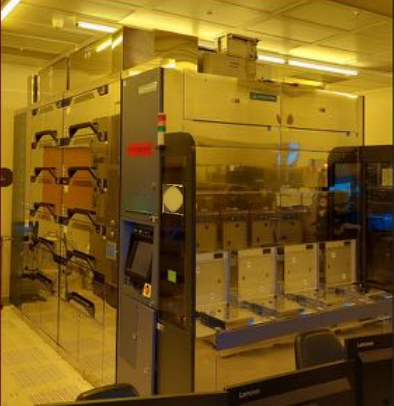
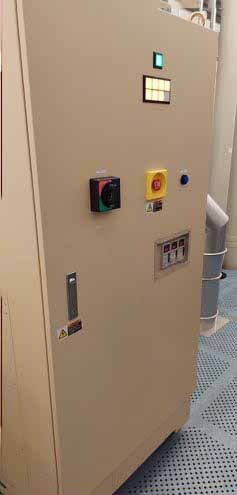
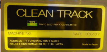
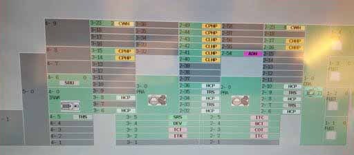
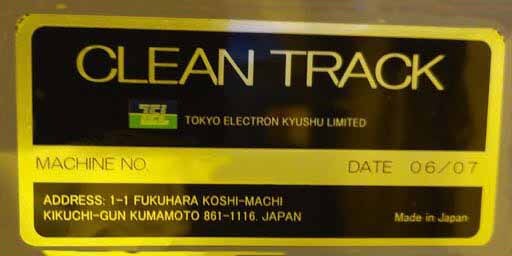
ID: 293671305
Wafer Size: 12"
Vintage: 2006
System, 12"
(4) Front Opening Unified Pod (FOUP) ports
(1) Chemical Robot Arm (CRA)
(2) Transfer (TRS) stations
(2) Process Robot Arms (PRA)
(2) Coater (COT) modules
(2) Bottom Coater (BCT) modules
(1) Wafer Edge Exposure (WEE)
(1) Cup Wash Station (CWH)
(1) Adhesion (ADH) unit
(1) Interface Transfer Cassette (ITC)
(2) Chill / Post Heat Plate (CPHP) units
(2) Low Temperature Hot Plate (LHP) units
2006 vintage.
TEL / TOKYO ELECTRON Lithius is a photoresist equipment used in lithography applications in the semiconductor industry. It is a resist film created from the mixture of photocurable compounds and a photostable medium such as an organic solvent. It is most commonly used for semiconductor patterns, including integrated circuits and MEMS. The first step in the process is to coat the substrate with the resist film. The film is prepared using a spin-coater which spins at a high speed to spread the resist evenly over the entire substrate. The resist is then imaged using ultraviolet light or other electromagnetic radiation, depending on the type of resist being used. After the image is exposed, it is developed by removing the exposed resist with a solvent. This reveals the pattern of the working layer on the substrate. The resist system is extremely sensitive to ultraviolet light and its chemical composition ensures it remains stable under harsh conditions. Its superior adhesion removes the possibility of substrate damage and minimizes contamination. The unit also has the ability to accurately detect defects and the ability to process large patterns. This makes it ideal for highly dense and precision-oriented patterning processes. The machine's excellent stability ensures the line widths and shapes remain consistent without shrinking or expanding over time. Since the resist film is ultraviolet light sensitive, it can also be used to examine samples by placing a sample on the film. This allows it to detect defects as small as 0.1µm or measure feature sizes with 0.01µm accuracy. It can also detect feature heights of different layers with an accuracy of only 0.001nm. The resist tool is also capable of processing high aspect ratio structures where the thickness can be as low as 1nm. This makes it an ideal choice for etched structures, especially in modern semiconductor lithography. The combination of the asset's sensitivity and stability makes it commonly used in a wide range of applications from wafer lithography to emerging MEMS structures and advanced packaging structures. The model is also used for metrology because of its high performance and repeatability. TEL Lithius is a unique photoresist equipment used in semiconductor and MEMS projects. Its ability to withstand harsh environmental conditions, excellent adhesion and accuracy make it an ideal choice for lithography processes and metrology applications. With the emergence of advanced MEMS patterning and packaging, the resist system has become an essential tool for creating the necessary detailed patterns for these emerging technologies.
There are no reviews yet