Used TEL / TOKYO ELECTRON Lithius #9111778 for sale
URL successfully copied!
Tap to zoom
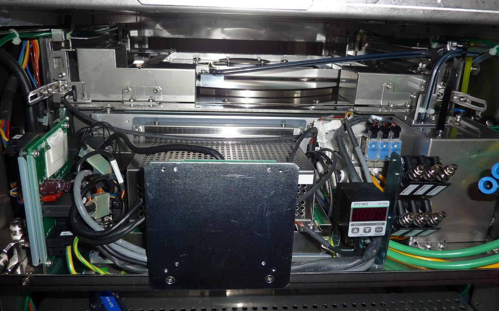

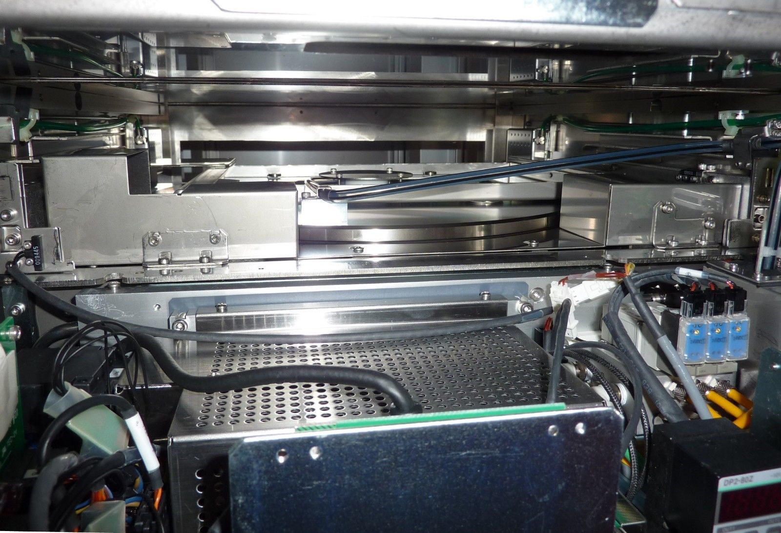

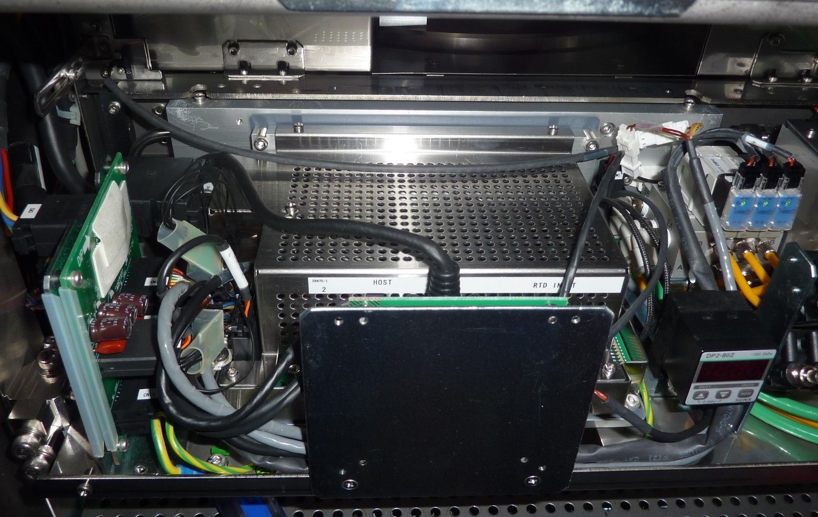

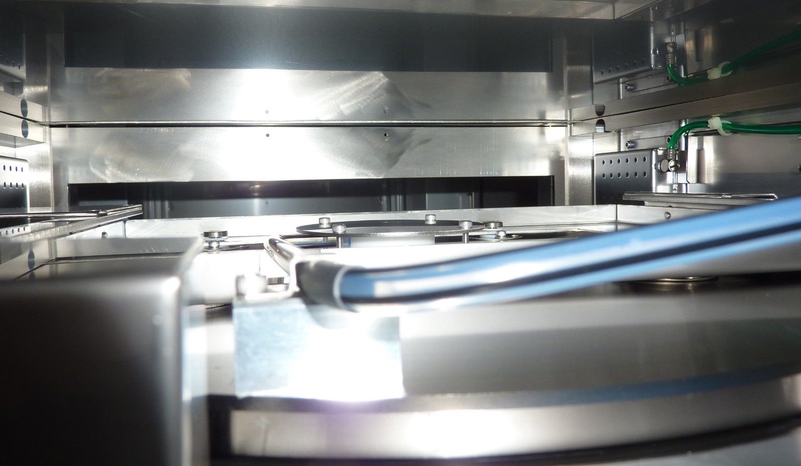


ID: 9111778
ADH Adhesion Process Station
BASE(HP) ASSY BACK, P/N: 5087-401692-19
PIN(ADH) ASSY, P/N: 5087-401608-12
SUPPORT(ADH) ASSY, P/N: 5085-407303-12
BASE(E-ADH) ASSY, P/N: 5087-401362-16
COVER(HP) ASSY, P/N: 5085-407301-12
PLATE(ADH) ASSY, P/N: 5085-402644-12
CHAMBER(ADH) ASSY, P/N: 5085-407298-13
COVER(ADH)ASSY BACK, P/N: 5085-408278-14.
TEL / TOKYO ELECTRON Lithius is an advanced photoresist equipment designed for use in the manufacture of semiconductor devices. It is designed to provide high quality patterning performance with low costs and high throughputs. The system utilizes a lithography technique called optical photolithography. This is a process involving the projection of light through a mask to produce patterns on the semiconductor material. TEL Lithius unit is equipped with an advanced optical source which emits ultraviolet (UV) light. This UV light is directed through a light mask onto a photoresist-coated semiconductor material. The photoresist layer is photosensitive and will change its structure when exposed to the light, creating a pattern. This pattern can then be developed and transferred onto the semiconductor material. The machine features an advanced optical illumination tool, a three-degree-of-freedom (3-DOF) alignment module, an advanced wafer scan, and an improved resolution of features, up to 65nm. The asset is capable of producing high-precision patterns with line widths of 1-2um, as well as completely eliminating stitching effects. It also has an advanced photoresist control model that can precisely manage the temperature, composition, and viscosity of the photoresist layer. The equipment also has an auto alignment system that ensures accurate alignment and precise patterning on various types of materials. It has a specialized die-to-die correction unit that can effectively eliminate any artifacts or irregularities created during the process. In addition, the machine has a deposition tool for the addition of protective layers over the patterned surface of the substrate. The asset is capable of running multiple processes simultaneously and is compatible with most mask aligners and wafer steppers. It is also capable of handling large and complex designs with multiple layers and features. Overall, TOKYO ELECTRON Lithius model is designed to provide a cost-effective solution for both high-precision patterning and the production of semiconductor devices.
There are no reviews yet
