Used TEL / TOKYO ELECTRON Lithius #9111797 for sale
URL successfully copied!
Tap to zoom



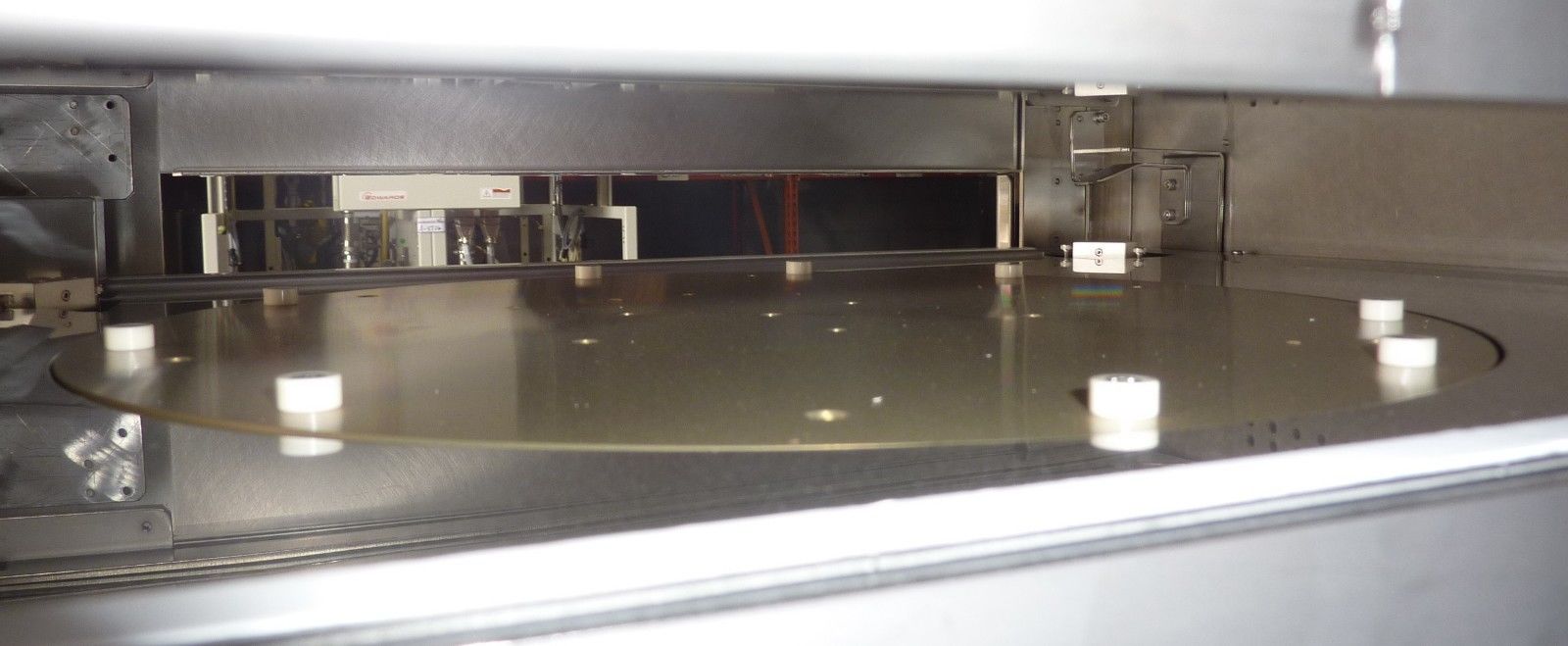


ID: 9111797
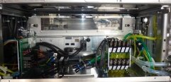
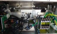
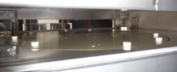
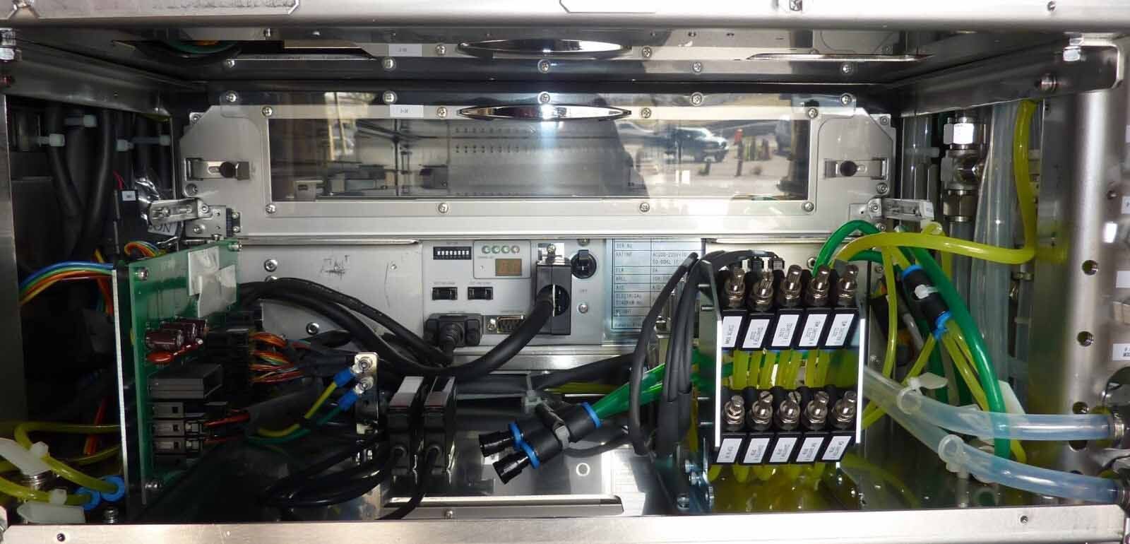
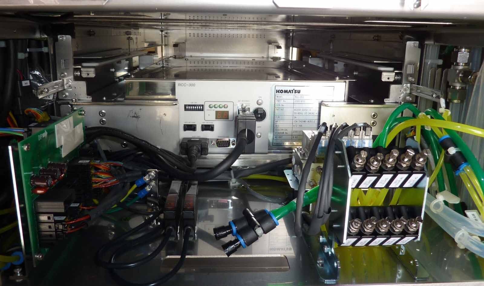
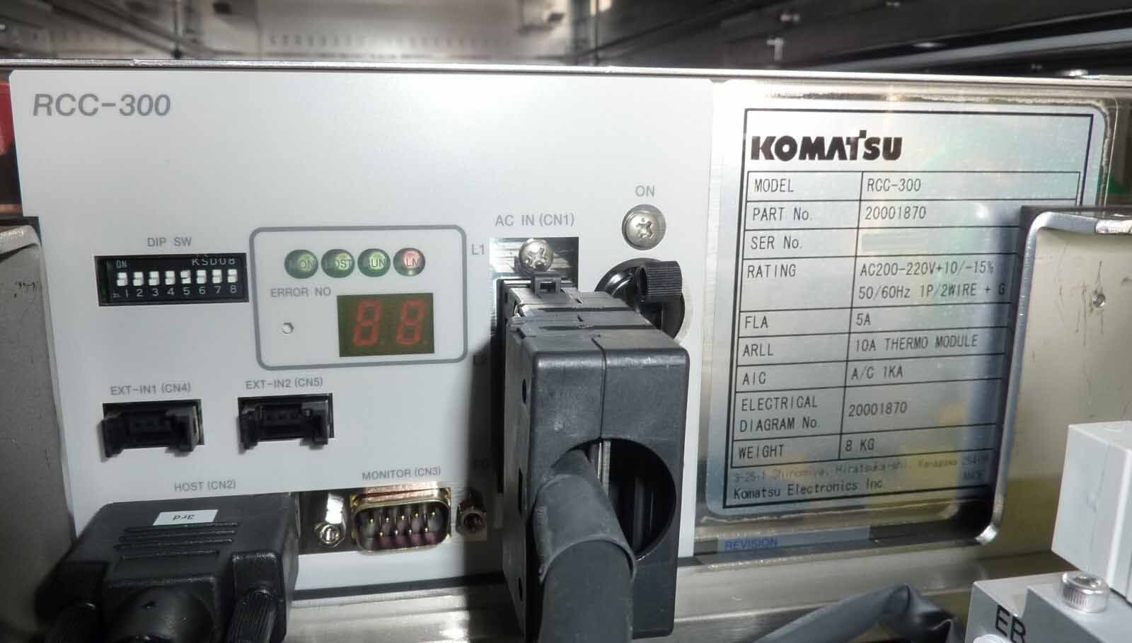
CPL Chilling Hot Plate Process Stations
BASE ASSY FRONT, P/N: 5087-402532-13
BASE ASSY MID, P/N: 5087-401685-19
BASE ASSY BACK, P/N: 5087-401686-17
BASE(CPL)ASSY SUPPORT, P/N: 5085-408084-11
GUIDE(10) ASSY, P/N: 5085-404679-12
COVER(CPL) ASSY BACK, P/N: 5085-408086-13
BRACKET(DSW)ASSY, P/N: 5087-402531-13.
TEL / TOKYO ELECTRON Lithius is a state-of-the-art photoresist equipment. Photoresist is a photosensitive material used in the manufacture of electronic circuit boards and semiconductor devices. The Photoresist System consists of 4 primary components; the Pulsed Excimer Laser, the Detector Module, the Polarizer Optics and the Wafer Stage. The pulsed excimer laser is a specialized unit that uses ultraviolet light to expose the desired pattern onto the photoresist coated wafer. The laser light induces a chemical change in the photoresist which determines the response of the photoresist to subsequent processing. The detector module is composed of a processor and two photo detectors. The processor processes and interprets the vector data sent from the host computer to determine the vectoring direction and amount of exposure. The two photo sensors measure the linear movement of the laser across the wafer surface and ensure that the entire surface of the wafer is exposed evenly. The polarizer optics is a device used to control the direction of the laser light beam. The optics contain several lenses and filters that can be adjusted to focus the beam on the desired pattern. This ensures that the pattern is exposed accurately and with the correct intensity. The wafer stage is a motion control machine used to accurately position the wafer beneath the laser. It is equipped with servo motors and encoders to control the XYZ positioning of the wafer. The stage has the ability to rotate the wafer for different orientations and its orientation can be changed rapidly to minimize the exposure time. TEL photoresist tool is one of the most advanced systems available and is used to manufacture advanced integrated circuits. The asset offers excellent speed and accuracy for creating complex patterns with superior edge resolution. It provides excellent reliability and is ideal for high volume production.
There are no reviews yet
