Used TEL / TOKYO ELECTRON Lithius #9185423 for sale
URL successfully copied!
Tap to zoom


ID: 9185423
Wafer Size: 12"
Vintage: 2003
(2) Coater / (3) Developer systems, 12"
Coaters:
(8) Resist nozzles
With (2) temperature controllers
Touch filters for resist / Solvent
Mass flow controller
Developers:
NLD Nozzles
With (3) temperature controllers
(3) PRD Nozzles
Touch developer filter
Thermo controller unit (TCU) inside track
Single block track
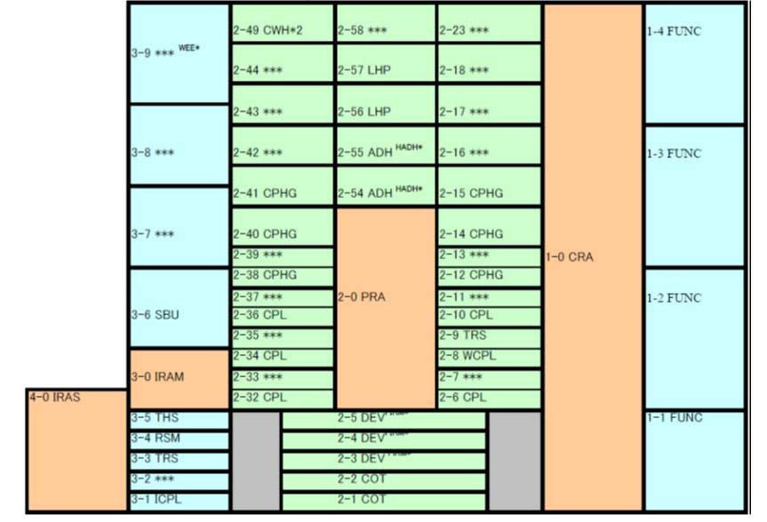
(4) Blocks interfaced / Wafer transfer robot arms:
Carrier
Process
Stepper interface main
Stepper interface sub
(4) Cassette FOUP designs
SECSI/II / HSMS / GEM Interface
Interface: NIKON S308
(2) Adhesion process stations (ADH)
(5) Chill plate process stations (CPL)
Transfer chill plate (WCPL)
(2) Low temperature hot plates (LHP)
N2 Purge capability
(6) Precision chilling hot plate process stations (CPHG)
Wafer edge exposure system (WEE)
Buffer cassette, 3"-6"
Hard disk not included
Sub components:
Temperature / Humidity controller
(2) Chemical cabinets
AC Power box
2003 vintage.
TEL / TOKYO ELECTRON Lithius is a photoresist equipment used for the imaging process in semiconductor device fabrication. It is an advanced tool for the creation of circuit patterns with an extremely fine resolution. The system uses a combination of ultraviolet (UV) light and solvents to remove the photoresist material in projected areas of a photomask. Photomasks are used to lay down a design pattern onto the substrate and are extremely fine in resolution compared to other lithography techniques. Photoresist, a photosensitive material applied onto the substrate, is used to etch the pattern onto the wafer or board. The resist material is then chemically removed from the substrate using solvents in order to reveal the pattern. TEL Lithius unit is designed to allow for precise control over the resist exposure process. It has a closed-loop machine to accurately detect when the process is complete, and includes an advanced stage control tool for automatically adjusting to the substrate's surface during the resist exposure process. The asset also offers several advantages. It is incredibly fast, with an exposure time of just 2.6 seconds for a full-length wafer. It has a very low thermal impact, so semiconductor devices do not experience any adverse effects from the exposure process. It is also designed for compatibility with a wide range of photoresist materials, so the model can be used for the development of extreme-resolution patterns. In addition to these features, TOKYO ELECTRON Lithius equipment is highly efficient. It offers a low power requirement and high throughput, allowing for the production of many devices in a short amount of time. It also has a low maintenance cost, as the system requires minimal maintenance while producing high-quality results. Lithius unit is an ideal choice for early-stage and production-level semiconductor device fabrication. Its advanced imaging technology and wide compatibility with photoresist materials make it an optimal choice for the development and manufacture of cutting-edge semiconductor devices.
There are no reviews yet